Introduction
The size of the VCSEL market is increasing and there is a pressing need to demonstrate high volume, high quality manufacturing. One of the most critical steps in manufacturing VCSEL is the formation of apertures. Aluminium rich layers are oxidised in a furnace at a high temperature under an oxygen rich atmosphere. The dry etching process of the p mesa then aims to expose the Aluminium rich layer before the oxidation.
The location of the aperture within the layer stack will depend on the design selected by VCSEL manufacturers and targeted electro-optical performance. In order to allow VCSEL suppliers to manufacture a specific design, the dry etching process must therefore be capable of stopping at any layer within the epitaxial stack. Layer by layer etching must be demonstrated across full wafers with precise control at the final layer.
Conventional time controlled etch processing is capable of supporting highly reliable manufacturing, however, endpoint techniques enable a tighter distribution of etching depth to a target layer by allowing for run-run etch variations as well as variations in the incoming material target thicknesses. Existing endpointing approaches have been tailored to meet the high volume, high yield requirements of VCSEL manufacturing. By combining strong process expertise and deep device understanding, Oxford Instruments Plasma Technology has developed advanced plasma processing solutions to enable current and future VCSEL designs.
Dry Etching of DBR Stacks
The DBR structure is made of GaAs/AlGaAs pairs with varying Al content. The layer stack is commonly dry etched using ICP – RIE mode using a chlorine based chemistry. Chlorine is reactive with Gallium, Arsenide as well as Aluminium and forms volatile by products at the processing temperature.
To expose the required layer, the etching depth has to be controlled precisely during the etching process and stop with optimal accuracy. Depending on the design of the laser, the etching might stop either on top or below the active region (QW cavity in Figure 1).
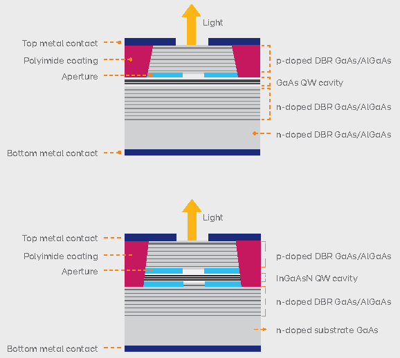
Fig. 1 — Oxide confined design variation 1 (top) and 2 (bottom).
On designs using AlAs layers in the n-DBR, these layers cannot be exposed during oxidation as they would oxidise faster than the AlGaAs layers and could cause blocking of the electron injection from the metal contact into the active region. They would also reduce the heat dissipation out of the active region. For inter-cavity contacted VCSELs, the end layer must also correspond to a specific interface to form ohmic contacts.
Conventional Laser Reflectometry
Laser reflectometry is commonly used in nanofabrication to monitor the etching depth while processing.
This method provides in situ real time monitoring by tracking the reflectance of a laser beam directed at the surface of the wafer.
When etching, the incident light is partially reflected and partially transmitted at the top interface of the film. The transmitted light continues through the film, reflects at the film/substrate interface, and returns back. Depending on the optical path length in the film, this results in constructive or destructive interference (or more commonly part way in between). As the film is etched, the interference condition changes, passing through positions of perfect constructive and destructive interference. The result is an oscillating signal shown in Figure 2 where an interference cycle corresponds to a particular depth, D, depending on the wavelength of the laser, λ, and the refractive index, n, of the material being etched.
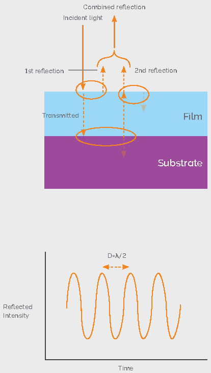
Fig. 2 — Principle of laser reflectometry.
An example of laser signal trace is given in Figure 3 when etching through a pDBR, QWs and few pairs of an nDBR of a VCSEL epitaxy wafer.
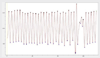
Fig. 3 — Reflectivity as a function of etching depth for mesa etch.
This technique is efficient at tracking the reflectance at a single point on the wafer, typically of the order of 60 µm in diameter, and in providing real-time etch rate information, however, information on how smaller features are etching is limited and there is no monitoring of the cross-wafer performance. It also requires auto focusing of the laser beam and pattern recognition to achieve maximum reliability or a dedicated larger feature to be included on the wafer.
The wavelength of the laser must be carefully selected in order to obtain the maximum signal intensity and the best determination of endpoint – in some cases using a longer wavelength with lower depth resolution for enhanced amplitude. The optimum wavelength corresponds to the wavelength the DBR are designed for i.e. the wavelength of the laser itself. However, the most common wavelength available and used in nanofabrication is 670 nm. For some designs, interference patterns can cause layers within the stack to not be detected or show low peak reflectance. Near infra red (NIR) wavelengths (e.g. 905 or 980 nm) offer lower attenuation in GaAs and can be useful for some applications.
Modelling of traces is given in Figure 4 for a DBR stack with a GaAs cap followed by the first confinement layer in quantum wells.

Fig. 4 — Modelling of reflectance spectra (top) and corresponding laser trace when using 670 nm laser (middle) versus 900 nm (bottom).
Optical Emission Spectroscopy Supports High Volume Production
To provide fine control of the end layer, the etching depth can also be monitored using optical emission spectroscopy (OES). In the plasma discharge, excited atoms and ions gives a unique emission spectrum specific to each element. Thus, a single element generates numerous characteristic spectral emission lines. While processing, the variation of the concentration of species in the plasma can be tracked. It is possible to track either a single element or a combination of elements and peaks to obtain a good endpoint signal. The technique is looking across the plasma above the wafer — it effectively monitors the progress of the etch across the whole wafer. This technique can be set to automatically endpoint a process by monitoring either a single line intensity or several lines combined using mathematical equation.
The trace observed will be dependent on the uniformity of the etching process as well as the footing. The strongest signal oscillation will be obtained when etching a single layer at the time, across the whole wafer. This technique can therefore only be enabled by very good uniformity of the etching depth across the wafer and ultra-low footing, ideally below the thickness of a single layer in the DBR pairs. These processing conditions are consistent with demonstrating high volume, high yield manufacturing capability.
An example of OES trace achieved using a PlasmaPro 100 Cobra 300 is given in Figure 5. In this case, OES was used to track the oscillation in the concentration of Gallium as we etched through the various layers of the DBR. This OES trace was captured for a sloped mesa profile with a uniformity of the etching depth across wafer within ±1%. As seen on the trace, each oscillation is clearly defined. Each oscillation corresponds to a pair of the DBR structure and the process can be set to stop on any of these peaks by tracking the first derivative of the signal.
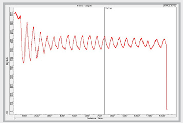
Fig. 5 — OES trace of Gallium line for a sloped mesa. Within wafer uniformity ±1%.
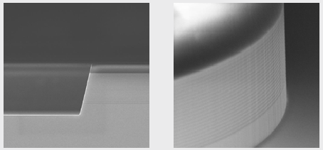
Fig. 6 — Tapered profile (left) and vertical profile mesa (right).
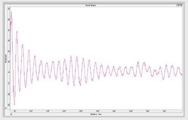
Fig. 7 — End pointing p mesa etching of 150 mm wafer using Oxford Instruments' solution.
Conclusions
We have developed advanced plasma processing solutions to deliver the device performance and yield demanded by the VCSEL market. We have demonstrated high precision technique for manufacturing VCSEL mesas. The VCSEL end pointing solution developed has been successfully applied to wafer sizes up to 150 mm and is compatible with high volume, high yield manufacturing. The fine control of the end layer is supported by excellent process uniformity and low footing along with tailored signal processing.
Whether OES or laser reflectometry is the best solution depends on the specific etch process performance and epilayer structures. OES in general, where it gives a clear signal, is preferred for production as it does not require manual intervention and it is based on the whole wafer etch performance rather than a single point.

