Introduction
As semiconductor devices continue to decrease in size to improve performance and take advantage of advances in fabrication techniques, there is a need to analyse both their structure and chemistry at ever increasing resolution. Typically this requires the use of TEM for metrology and failure analysis. Using ultra-high resolution FEG-SEM, low kV imaging and the X-Max® Extreme EDS detector we demonstrate the ability to retain some of this high resolution analysis in the SEM. This allows for better targeting of resources and increased throughput of analysis.
Identifying Components
Due to the nature of bulk specimens, the spatial resolution of imaging in the SEM is limited by the interaction volume of electrons within the specimen. The same is true for the generation of characteristic X-rays. However, the depth from which X-rays can escape a specimen is greater than that of secondary electrons. As a result X-ray map spatial resolution is normally worse than that of a secondary electron image. To limit the interaction volume in bulk specimens it is becoming standard practice to image at increasingly lower electron landing energy as shown in Fig. 1a.
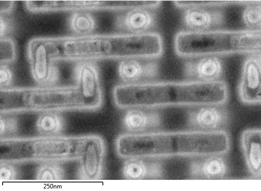
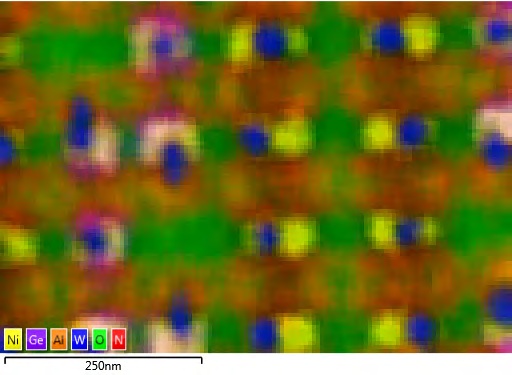
Fig. 1. a) secondary electron image and b) layered EDS map of a complex 3D semiconductor structure acquired at an incident electron energy of 3kV.
At 3 kV the interaction volume is limited to <50 nm in both depth and lateral dispersion. This energy is useful for mapping semiconductor devices as spatial resolution is high while there remain characteristic X-ray lines for all the elements in the specimen. Mapping for six minutes at 3 kV yields the results shown in Fig. 1b. The specimen mapped in this case is complex with buried layers close to the surface and feature sizes smaller than 10 nm. Using X-Max Extreme and AZtecEnergy TruMap the majority of the structure is resolved. Common peak overlaps such as Si K / W M are deconvoluted and variations in X-ray background due to element mass number are removed. From the X-ray map the regions of Si and N are clear but what is most striking is the ability to resolve the central W regions of the multilayered node structures in the device as well as showing the difference between those structures with Ni/Ge (pink in Fig. 1b) surrounds and those with just Ni (yellow).
The fidelity of this analysis can be improved even further by using linescans in addition to X-ray maps. Linescans in AZtecEnergy offer all the same real time processing of X-ray maps so that background and peak overlap artefacts are removed. Using line scans improves sensitivity by focusing data acquisition in a much smaller number of pixels. This is particularly useful when measuring thin layers such as the TiN boundaries to metallic regions within this specimen. The EDS linescan (Fig. 2) even highlights information that is not clear in the electron image. The W area on the left hand side of the line scan is bounded by a thin TiN region (A). This layer although only 4.6 nm in the electron image can be resolved in the EDS line scan due to the improved sensitivity and the excellent spatial resolution possible with this technique. The similar region on the right hand side of the line scan (B) is without this layer, as is shown by the missing Ti and N signals.
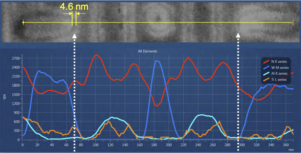
Fig.2. EDS linescan acquired at 3kV and electron image of the region scanned.
Due to the large solid angle of X-Max Extreme it is possible to continue decreasing electron landing energy. The Monte Carlo simulations shown in Fig. 3 show how the interaction volume in pure Fe would change as the incident electron energy is reduced from 5 kV to 1 kV.
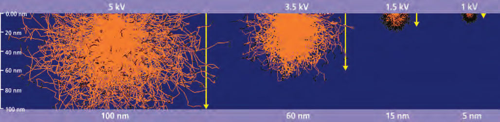
Fig. 3: Monte Carlo simulations of interaction volumes for the Fe Lα X-ray line in pure Fe for electrons with landing energies of 5kV, 3kV, 1.5kV and 1kV. Red indicates electron paths which would result in the emission of X-rays, black indicate electron paths where an X-ray would not be emitted.
Due to the complex 3D sample structure, the collected spectra include information from buried layers. However, the Monte Carlo simulations show that as the incident electron energy is reduced not only would the spatial resolution potentially improve but X-rays would be generated much closer to the surface of the sample giving a much improved surface sensitivity.
Therefore, the same analysis was repeated with an electron landing energy of 1 kV. Using a six minute map of a similar region we can directly compare the difference in resolution and surface sensitivity. Fig. 5 shows side by side maps of a number of elements in the specimen. The difference in the elemental maps for light elements is immediately noticeable; the spatial resolution of the N map and the depth resolution of the O map are greatly improved. The 1 kV O K map reflects the structure observed in the electron image and not the structures buried below. Some heavier element maps like Ti also show a large improvement in sensitivity. The 1 kV Ti map correlates more closely with the Ti signal shown in the linescan (Fig. 2). Moving to 1 kV for X-ray analysis does however limit the number of characteristic X-ray lines available for elemental analysis. For some elements, Ni – Rb, there is no characterised line, while for others these X-ray lines are characterised but rarely used for analysis. Fig. 5(d & e) shows that we can move away from conventionally used lines like W M and instead use W N (210 eV) and use Si L (92 eV) instead of Si K.
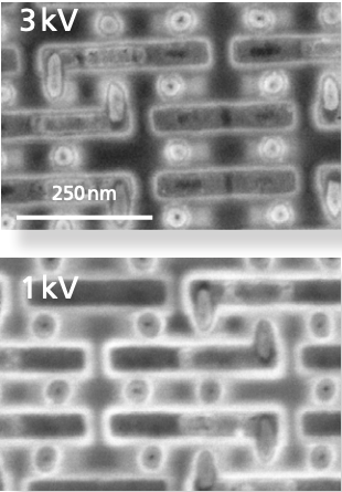
Fig 4. a) secondary electron image of semiconductor device taken at 3 kV. b) a secondary electron image of a similar region of the same device acquired at 1 kV
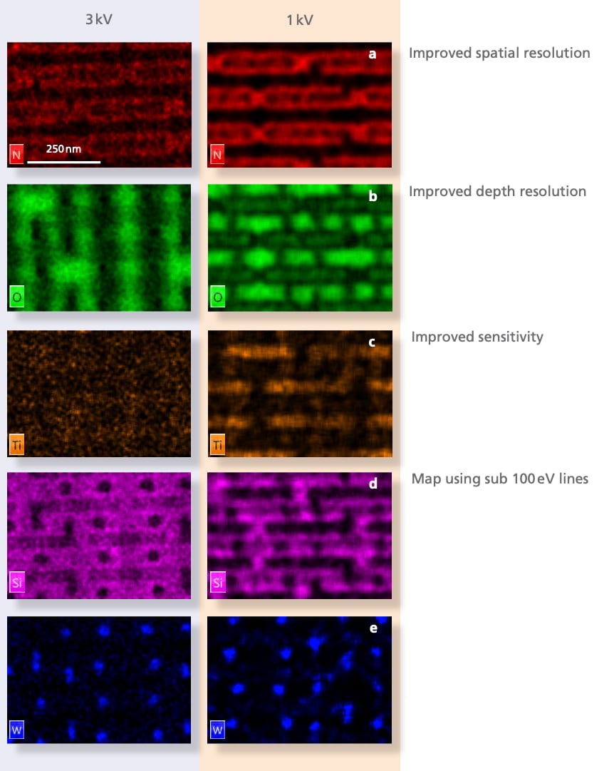
Fig. 5. a-e) EDS maps for N, O, Ti, Si and W collected at incident electron energies of 3kV and 1kV .
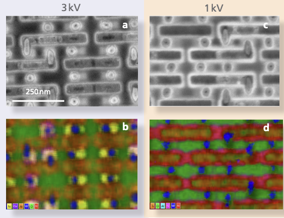
Fig. 6. Secondary electron images (a and c) and layered EDS maps (b and d) at 3kV and 1kV respectively
Fig. 6 shows the layered maps created from the data in Fig. 5. The 1 kV map in Fig. 6d shows clear improvement of resolution of the N regions as well as the improved sensitivity to the surface composition of the specimen, especially O. The regions of Ge and Ni are conspicuously missing from the 1 kV map due to the lack of X-ray lines in this energy range. Comparison with the 3 kV map in Fig. 6b shows the relative positions of these regions. Viewing these two layered X-ray maps side by side allows complete understanding of the specimen from just two six minute SEM acquisitions using X-Max Extreme.
Conclusion
Using low kV SEM to analyse semiconductor materials can reveal information that would otherwise be indiscernible at higher kV. We have shown that by decreasing the incident electron energy the interaction volume in the sample can be reduced, improving both the spatial resolution and surface sensitivity of EDS analysis. We have also shown that it is possible to measure chemical information of many elements commonly used in semiconductor devices at 1 kV using extremely low energy X-ray lines. The results presented here show that with X-Max Extreme and ultra-high resolution FEG-SEM it is now possible to achieve results that show all elemental components and are comparable with TEM using just two six minute X-ray maps. With EDS maps and line scan resolutions of <10 nm now possible in SEM, failure analysis and metrology of semiconductor nanostructures can now be carried out on bulk specimens. This allows for a much more targeted approach to subsequent analysis steps using TEM or other techniques.

