Shaping the Future of Semiconductor Manufacturing with Oxford Instruments at SEMICON Japan 2026
Join Oxford Instruments at SEMICON Japan 2026, taking place 9-11 December 2026 at Tokyo Big Sight, and discover how our solutions are helping semiconductor manufacturers and researchers accelerate innovation from materials development to high-volume production.
Explore our comprehensive portfolio of plasma processing and advanced characterisation technologies designed to address the challenges of next-generation semiconductor devices, advanced packaging, power electronics, compound semiconductors, and emerging materials.
Our experts will be available to discuss how Oxford Instruments can support your fabrication and analysis requirements with solutions including:
- Atomic Layer Etch (ALE)
- Atomic Layer Deposition (ALD)
- ICP etch and deposition systems
- PECVD
- Plasma Polish Dry Etch for SiC processing
- Raman imaging microscopy
- Atomic Force Microscopy (AFM)
- Energy Dispersive Spectroscopy (EDS)
- Electron Backscatter Diffraction (EBSD)
- BEX (Backscattered Electron and X-Ray) technology
From precise etch, deposition, and material growth processes to advanced materials characterisation, our technologies help deliver the insights and process control needed to advance semiconductor research and manufacturing.
Experience Live Demonstrations
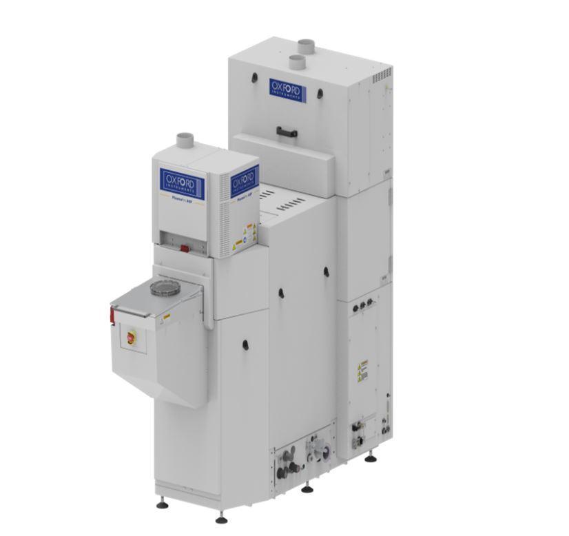
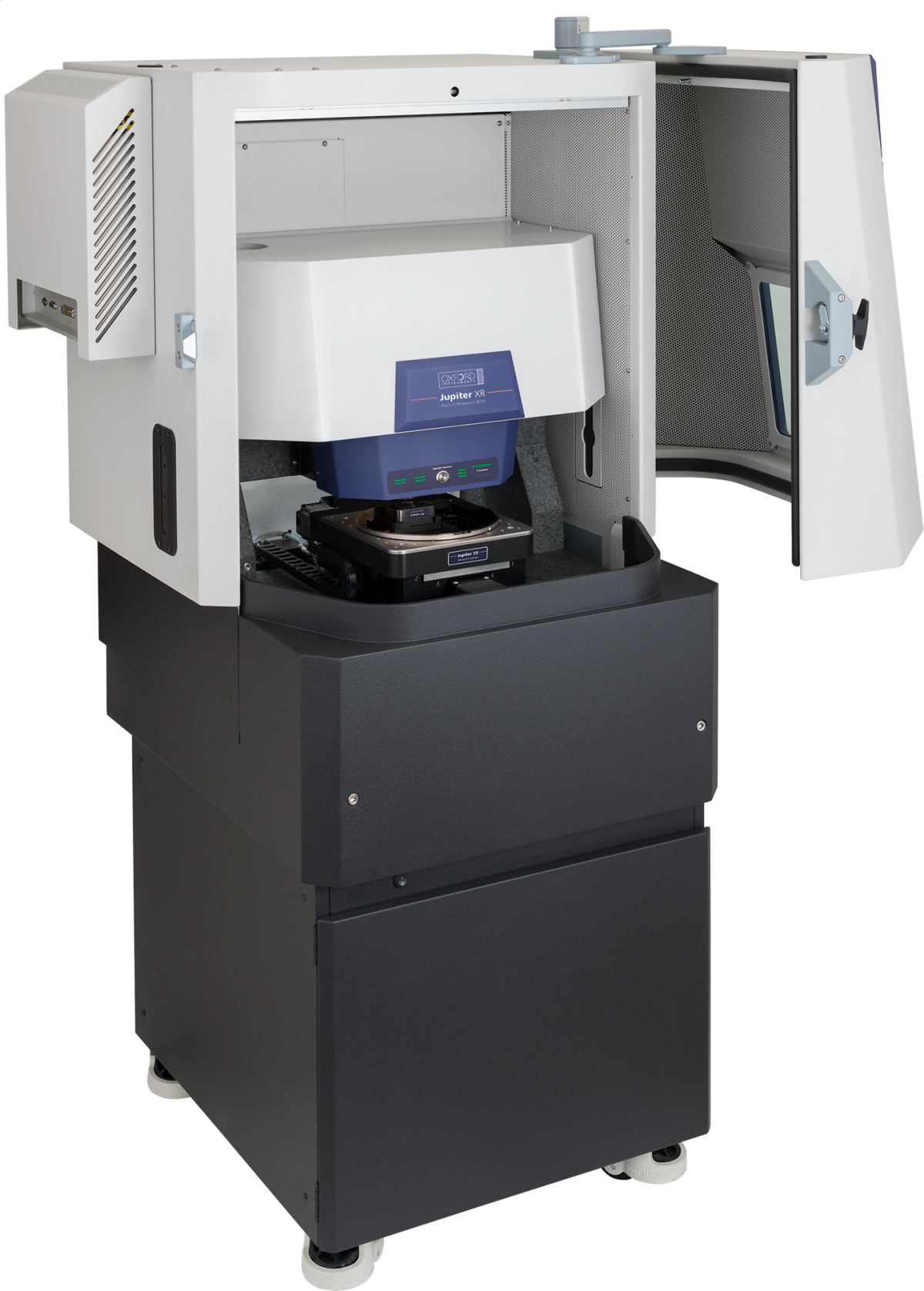
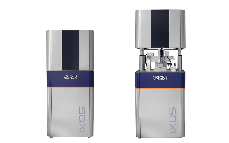
Don't miss live demonstrations of the Jupiter AFM and WITec 360 Raman Imaging Microscope at our booth. Experience our PTIQ Augmented Reality software demonstration and virtually explore the PlasmaPro ASP ALD system.
Discover how combining high-resolution surface metrology with Raman and photoluminescence analysis can provide deeper insights into material properties, process optimisation, and failure analysis. Learn how complementary characterisation techniques enable a more complete understanding of semiconductor materials and devices, helping to accelerate development and improve manufacturing outcomes. Book a live demonstration today.
Meet the Oxford Instruments team at Booth E3311 (East Hall 3) and speak with our experts about your latest challenges in semiconductor process development, materials analysis, and device characterisation. Schedule a dedicated meeting with us today!
For further information about the event, visit the Semicon Japan 2026 webpage.
Location
Tokyo Big Sight, Japan
Date
09-11 December 2026
Booth Number
E3311 (East Hall 3)
Registration for Semicon Japan 2026
Register Now
Schedule a meeting with us at the event. Please fill out the form below.
Book a meeting
See live demonstrations of Jupiter AFM, witec360 Raman imaging and PTIQ Augmented Reality software
Book an AFM, Raman and PTIQ demonstration