Meet Oxford Instruments at the event for electronics manufacturing in Munich, Germany (Booth 606 - Hall B1).
The Semicon Europa event is the largest European exhibition for electronics manufacturing and broadening the range of attendees across the electronics chain. Semicon Europa provides highly technical content specific to the type of industry. The main objective is to promote technological progress featuring the most advanced and innovative electronics manufacturing in Europe.
Advance your semiconductor fabrication and characterisation processes with Oxford Instruments’ full spectrum of solutions.
Achieve precise and consistent etch, deposition and growth of micro- & nano-structures and films, using atomic layer etch (ALE), atomic layer deposition (ALD), ICP (etch & dep), PECVD and Plasma Polish Dry Etch for SiC processing with our plasma technology solutions. Measure crystal homogeneity, material stress and strain in 3D with Raman imaging microscopy; characterise defects, roughness, elasticity and electronic properties using Atomic Force Microscopy (AFM); evaluate structure and elemental composition with the electron microscopy techniques: EDS, EBSD, and the revolutionary BEX (Backscattered Electron and X-Ray).
Our team is looking forward to meeting you at booth 606 (Hall B1) and discussing your current work and process challenges with you! For further information visit the Semicon Europa 2025 Program.
Interested in seeing more? You will have the chance to book a demonstration for our two new top products that were recently launch:
The witec360 Raman Semiconductor edition as well as our Jupiter Discovery AFM.
Book a demo
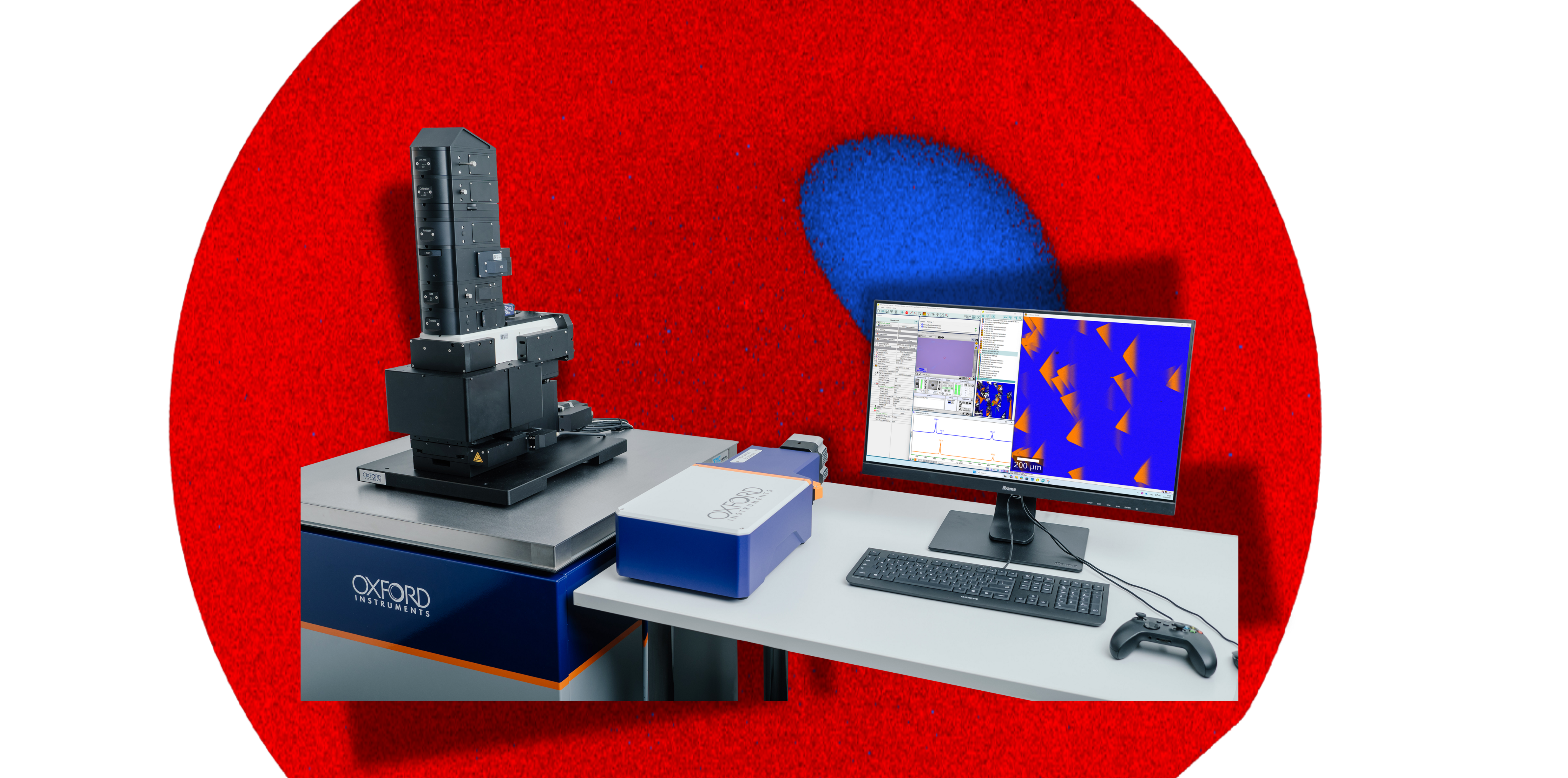
The witec360 Semiconductor Edition
is a high-end confocal Raman and photoluminescence (PL) microscope specifically configured for the chemical imaging of semiconducting materials.
- Full inspection of up to 300 mm
(12 inch) wafers
- Non-destructive characterization of crystallinity, polymorphism, defects,
strain and doping
- Analysis of wide-bandgap semi-
conductors and layered structures
- Surface analyses, depth scans and 3D imaging
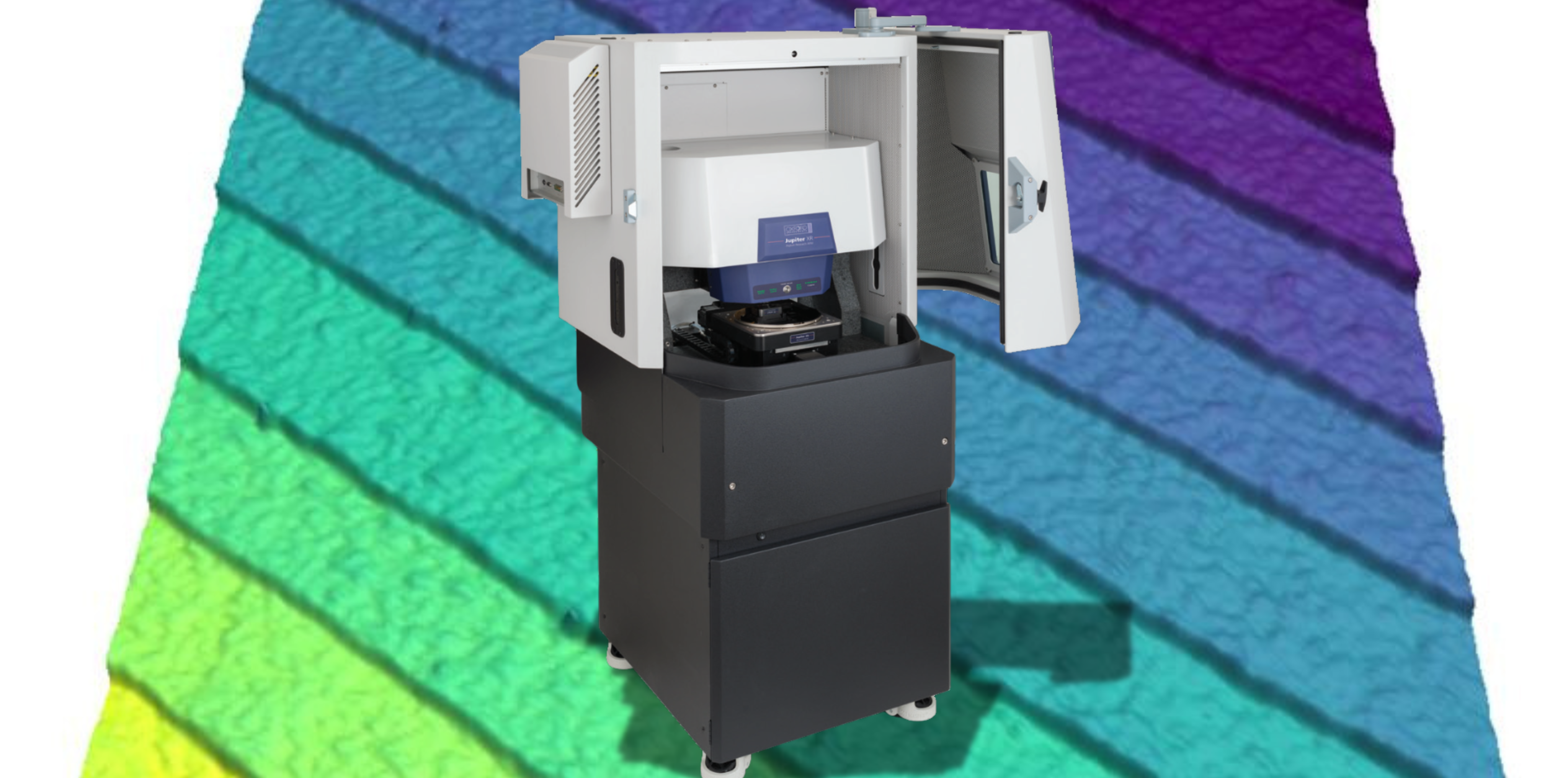
The Jupiter Discovery Atomic Force Microscope offers a unique combination
of best-in-class performance along with exceptional ease of use. Whether in aca-demia or industry, researchers expect high quality results with less training and effort.
- Next-generation design delivers the ultimate performance
- Optimized workflow for simpler and more productive user experience
- Unmatched configurability catisfies diverse research needs


