Recently, I was asked to analyse wires for quality control purposes. It was the first time I ever looked at wires, and I found it fascinating. In this blog, I would like to share the results with you, and I hope you find the data exciting, too.
The wires imaged and analysed below were not treated in any way (polished or coated) prior to analysis. The detectors used for this project were Ultim Max 170 mm2 and Unity. This is a very powerful combination of detectors, as Unity allows for the analysis of rough samples. Thus, collecting data without being affected by shadowing effects that conventionally positioned detectors would normally be affected by.
The wires analysed here failed, and the objective of the analysis in this case was to look for contamination and formulation inconsistencies or anything else that might have affected the production process.
There are 3 layers that could be immediately distinguished by analysis: Cu (top layer), Nb (middle layer), and Sn (core).
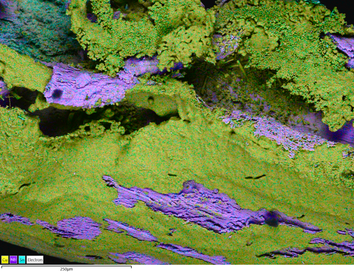
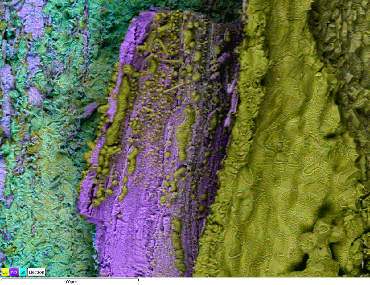
Figure 1: Zoomed out area. The edge of the wire surface can be spotted at the bottom left. You can see parts of the Cu layer missing, revealing the Nb later underneath.
Looking at the wire at a low magnification, the inconsistency of the Cu layer was obvious (Figure 1). It is inconclusive if the inconsistency caused the failure or if it was caused by failure.
There are also areas where damage on the Cu layer can be interpreted as the effect of bending (ridges and peeling of the Cu layer), potentially introduced when the sample was taken (Figure 2).
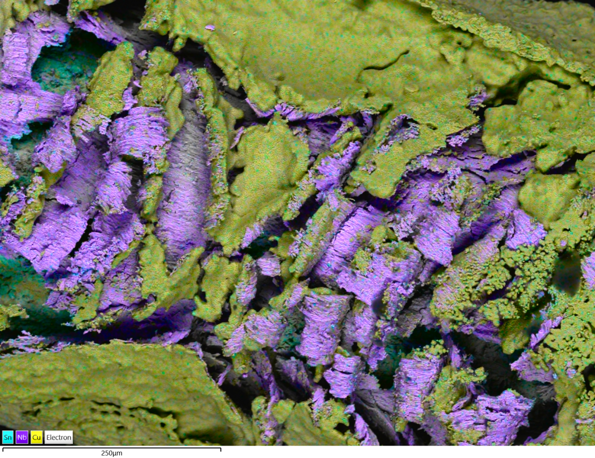
Figure 2: Damage on the top layer of the wire (Cu), revealing Nb (middle layer), and Sn (core layer). This image shows ridges and peeling of the top and middle layers, probably induced by bending.
Looking at the rough surface of the wire (Figures 1 & 2) at higher magnification, we can see more details on the exposed surface of each of the layers, side by side. It is noticeable that due to the damage the layers have unrolled and some parts have peeled off (Figure 3).

Figure 3: Different part of the wire (zoomed out). Acicular Cu on Nb layer. All 3 components of the wire (Cu. Nb, Sn) can be seen here side by side.
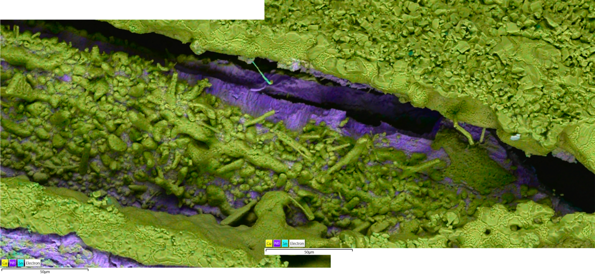
Figure 4 Cu textural change, The Cu layer texture ranges from almost planar to very rough, irregular, to lobe-like 3D structures. On the wire surface Cu appears continuous and the particles the layer is made of are very angular and tend to be symmetrical. The texture changes to fine-grained right below the top later, whereas at depth the Cu layer is comprised of irregularly shaped particles ranging from spherical, lobe-like to acicular grains, often discontinuous. Note the depth from which data has been collected despite sample topography.
Focussing on the Cu layer, different textures can be observed (Figure 4). The images of Figure 4 were taken from adjacent areas in an attempt to show the variation of textures within the Cu layer within a few microns. The images were taken at the same magnification and were overlaid using third-party imaging processing software. The Nb layer response to damage is quite different compared to the Cu layer; this might have happened because the Nb layer is under the Cu layer and might have been protected.
Lastly, there were areas where the wire core was totally exposed, with the Cu and Nb layer completely gone (Figure 5), resulting in the sample being slightly out of focus on the right.
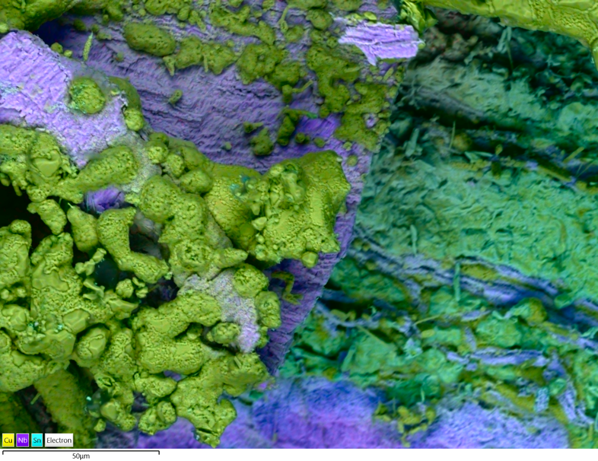
Figure 5: Rough wire surface. The Cu and Nb layer have completed peeled off on the right. Note that because of sample relief, the left part of the image is in focus whereas the right is slightly out of focus, because it is topographically lower; data was collected regardless of the height difference using Unity (BEX).
The synergy between Ultim Max and Unity is very powerful as imaging rough samples is facilitated and can be performed in high resolution. The customer gave their permission to use the data shown here but preferred to not disclose their identity and the full results of the analysis.
This a good example of analysing rough samples for routine work like QA/QC and even for R&D when it comes to failure analysis. The great advantage here is saving time as we don’t need to prepare the samples in order to image and analyse them. Contact us and find out how we can help you.