What is doping in the semiconductor world?
In semiconductor production, doping refers to the process of intentionally introducing foreign atoms to the regular crystal lattice of a semiconductor to produce dramatic changes in its electrical properties; creating n-type (extra free electrons) and p-type (deficiencies of valence electrons, called "holes”) semiconducting materials.
In this blog post, we will look at some data acquired from a gallium nitride (GaN), p-type semiconductor material - which is essential for both GaN-based electronics and optical devices. Such devices require both n-type and p-type materials, so that electrons and holes can be injected and transported to the active layer, where they recombine and emit light.
In GaN, n-type doping can be achieved by adding elements, such as silicon or germanium. Mg is the only viable dopant for the production of p-type GaN. That said, effective Mg-doping of GaN poses particular challenges because of the low chance of electrical activation. Overcoming this was crucial in the early development of blue LEDs (see later). In measurement terms, it is important to distinguish the density of Mg atoms introduced into the material and the resulting density of free holes (e.g. measured using the Hall effect).
I will also show results acquired on a Mg:GaN layer of 1 μm thickness that was grown on a nid-GaN buffer layer (1 μm), grown heteroepitaxially on sapphire. A number of Mg:GaN samples were grown by Drs. Chris Deatcher and Ian Watson using metalorganic vapour-phase epitaxy (MOVPE) at Strathclyde University, Glasgow with more details presented in Ref. [1].
We have employed WDS to analyse the GaN sample due to the superior detection limit of WDS compared to EDS; in this sample, Mg is present at a trace level (below 1.0 wt. %) which would be difficult to accurately measure with EDS. We will also compare the WDS data for the analysis of Mg to SIMS results, provided by the sample growers, in order to confirm the accuracy of the approach.
WDS results
The analysis of magnesium X-rays was performed with a thallium acid phthalate (TAP) diffracting crystal. The first action was to acquire wavelength scans to check we could clearly identify the Mg peak. The scan was collected using an accelerating voltage of 10 kV and a beam current of 40 nA and the acquisition time was 1 hour.
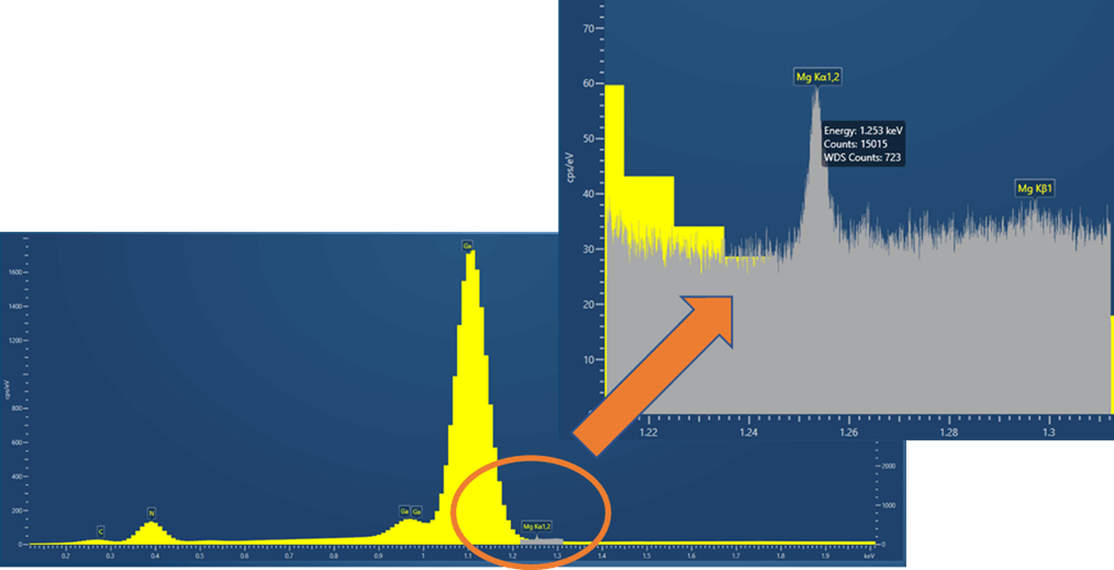
Figure 1. WDS scan of the Mg Kα peak using the TAP crystal in the Wave spectrometer
The WDS scan clearly confirms the presence of the Mg Kα peak at position 1.253 keV. Here we can see the true power of the WDS technique; the Mg peak is not even detectable in the EDS spectrum (yellow). Now that we have confirmed the existence of the Mg in a qualitative scan, we can continue with quantitative analysis. When measuring the relatively weak magnesium Kα peak, we have to pay very careful attention to the background. It is crucial to avoid any potential interference and achieve the most reliable background counts. In WDS, X-rays are counted at the position of the characteristic X-ray peak and at two background positions, usually close to and on either side of the peak position. An extrapolation is then made between the two measured background positions to determine how many counts are attributable to the continuum X-ray background at the position of the element-line peak, and these counts are then subtracted. To produce a quantitative result, the intensities of specific X-ray lines from different elements in the unknown sample are then compared to the intensity of the same element in a standard material of known composition.
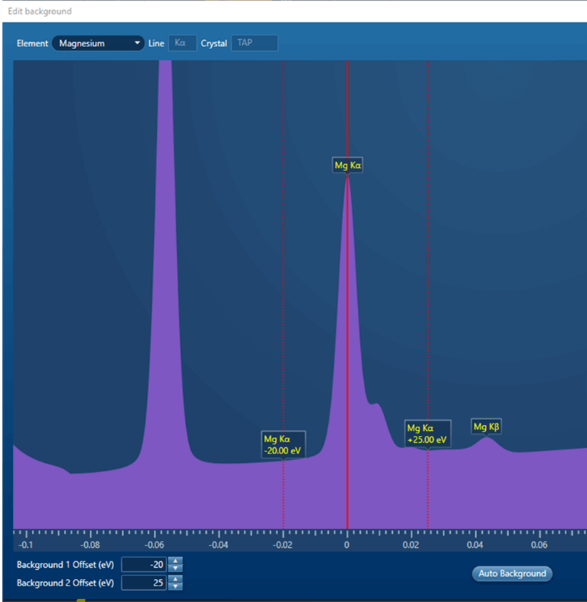
The AZtec Wave software offers a virtual WDS spectrum functionality where the user can use an auto function to set up background positions or manually adjust them. Care must be taken when choosing background positions for the measurement of Mg due to the Ga Lβ line being in close proximity to the Mg Kα line, and being significantly more intense.

Figure 2. The theoretical WDS spectrum modelled by AZtec prior to acquisition. The vertical red lines show the positions used for measuring the background intensities for the Mg Kα line.
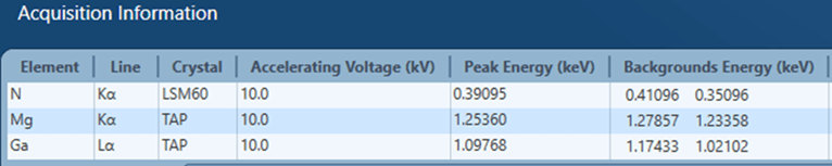
Compositional measurements were performed at an accelerating voltage of 10 kV (90% of the beam energy is deposited within a depth of ∼400 nm, determined using Monte Carlo modelling) and a beam current of 100 nA. Quantitative analyses involved signal acquisition for 120 s at the centre of the magnesium peak, while for the Ga and N measurement, the analysis time was set to 60 s. Due to the small signal intensity of the Mg Kα peak, a longer measurement time was needed in order to improve the counting statistics and signal-to-noise ratio. Even before starting data collection, based on measurement times and absorbed current, software will calculate target wt% sigma. A GaN standard was used as a standard for Ga and N, while a MgO standard was used for Mg. In order to avoid any possible charging effects on the sample surface, the sample was coated with a thin layer of carbon (∼15 nm in thickness). The sample was measured at nine different analysis points.

Figure 3. Acquisition setup for measuring Mg:GaN sample
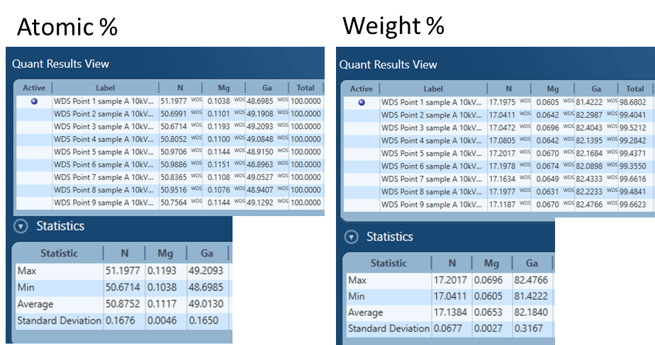
Figure 4. Quantitative results for the Mg:GaN sample determined by WDS
The average magnesium concentration measured in the sample corresponds to a mass percentage of 0.0653%, equivalent to a concentration of 9.8 × 10¹⁹
cm-3 which shows good agreement with the SIMS values of 9.5 × 1019 cm-3 and EPMA values of 9.4 (±0.2) × 1019 cm-3 published in [1]. Results show it is possible to use SEM-based WDS to measure highly doped semiconductor layers.
You might be asking why we want to analyse doping levels in semiconductors?
We analyse doping levels in semiconductors because it is important to know the amount of trace impurities that are incorporated into semiconductors, as they can significantly affect the electronic properties. In addition, unintentionally incorporated impurities can generate defect states inside the bandgap or non-radiative recombination centres which will affect emission properties of the device. This information can also help the growers to optimise their growth process.
In what type of device is this material used for?
Theses types of GaN:Mg layers are employed in p–i–n light emitting diode (LED) structures, in which the topmost layer often comprises 150–200 nm of highly doped GaN:Mg.
Another question that probably comes to mind is why we would use WDS to measure doping when there are other established methods?
It is true that the usual technique used to measure Mg concentration in nitrides are spectrometry techniques, such as SIMS and glow discharge mass spectroscopy. However, there are some major advantages to using the SEM-based WDS method including:
- The non-destructive nature of the technique
- The more affordable instrumentation
- The possibility to produce quantitative multi-element analysis
- More affordable standards for quantification
- It allows simultaneous acquisition of other analytical signals in the electron microscope
Additional Background - If you are interested to know more
Let’s go back into the past and talk a bit about how it all started. In the 1970s and 1980s light-emitting diodes (LEDs) were limited to just a few colours. There were green, yellow and red LEDs fabricated from widely studied semiconductor compounds. The blue LEDs were still not available and gallium nitride (GaN) was one possible candidate for creating them. The first functioning GaN:Mg LED was demonstrated in 1972 but it suffered from relatively low efficiency due to imperfections and defects and they were far from being ready for commercial production [2].
A first breakthrough in growth technology came in 1986, when Isamu Akasaki and Hiroshi Amano from Nagoya University in Japan developed a suitable growth method and device structure based on a chemical vapour deposition technique. However, another unresolved complication was the growth of the p-type layer [3]. The issue was related to neutralisation of dopants (usually zinc or magnesium) which would hamper the efficiency of the LEDs. Akasaki and Amano noticed that when GaN doped with zinc was measured in an electron microscope, the brightness of their LEDs is improved. This suggested that electron irradiation improved the p-doping – an effect that was later explained by Nakamura [4]. This breakthrough invention enabled conversion of compensated Mg-doped GaN to conductive p-type material.
In 1993, Nakamura developed the thermal annealing technique to remove the detrimental hydrogen that deactivated the p-type dopants, leading to the first high-efficiency blue LED presented in 1994 [5]. For their invention, Nakamura, Akasaki, and Amano were awarded the Nobel Prize in Physics in 2014 [6].
For anyone intrigued to learn more about this invention, I would highly recommend watching the talk given by Dr. Nakamura about the Invention of High Efficient Blue LEDs and Future Lighting, which can be viewed here.
It is captivating when you think about it, that Akasaki and Amano noticed that the brightness of their LEDs improved after being irradiated by the electron microscope, and now we are using the electron microscope again to analyse the very same type of samples. Truly fascinating!
Acknowledgment
The author would like to thank Dr. Ian Watson from the Institute of Photonics, University of Strathclyde and Prof. Robert Martin University of Strathclyde, Glasgow for providing GaN:Mg sample used for the measurements.
Bibliography
- Deatcher, C., et al., Wavelength-dispersive x-ray microanalysis as a novel method for studying magnesium doping in gallium nitride epitaxial films. Semiconductor Science and Technology, 2006. 21: p. 1287-1295.
- Maruska, H.P. and W.C. Rhines, A modern perspective on the history of semiconductor nitride blue light sources. Solid-State Electronics, 2015. 111: p. 32-41.
- Heber, J., Nobel Prize 2014: Akasaki, Amano & Nakamura. Nature Physics, 2014. 10(11): p. 791-791.
- Nakamura, S., et al., Hole Compensation Mechanism of P-Type GaN Films. Japanese Journal of Applied Physics, 1992. 31(Part 1, No. 5A): p. 1258-1266.
- Nakamura, S., T. Mukai, and M. Senoh, Candela‐class high‐brightness InGaN/AlGaN double‐heterostructure blue‐light‐emitting diodes. Applied Physics Letters, 1994. 64(13): p. 1687-1689.
- Nakamura, S., Background Story of the Invention of Efficient InGaN Blue-Light-Emitting Diodes (Nobel Lecture). Angewandte Chemie International Edition, 2015. 54(27): p. 7770-7788.