13th January 2021 | Author: Dr Rosie Jones
AZtec LayerProbe is a software solution that utilises sample analysis by Energy Dispersive X-ray Spectrometry (EDS) to determine both thickness and composition of thin layers, coatings, and films. Many of the samples imaged and analysed in the SEM have layered structures. For example, items such as electronic circuitry, solar cells, or even jewellery, may include thin films and it is often necessary to understand exactly what those layers are made of and how thick they are. This information can be useful for various purposes, including:
- Materials characterisation
- Quality control
- Fault finding
An electron beam hitting the surface of a sample inside a SEM has an interaction volume, the size of which depends on the acceleration voltage being used. When a sample contains thin layers close to the surface (maximum depth of 2 – 4 µm below the surface, depending on the acceleration voltage being used and the density of the layers) this interaction volume crosses multiple layers. The resultant EDS spectrum includes signals from all the layers that have been crossed making it possible to determine the thickness and composition of those layers. For more background information on LayerProbe, please refer to an earlier blog post written by my colleague Matt Hiscock, or our LayerProbe product page.
My ten top tips and tricks for successful analysis and results using AZtec LayerProbe
*Listed in the order that they would be applied as you work through an analysis in LayerProbe.
1. Sample Preparation
Sample preparation – as with normal EDS analysis, for good quantitative compositional analysis (of which LayerProbe is an example), the sample should ideally be flat and conductive. If the sample is not conductive, a conductive coating such as carbon should be applied to stop the sample charging under the electron beam. If a conductive coating is applied, then this should be treated as a separate layer and information on this should be added into the described model (see figure in point 4).
2. Sample Setup
Sample setup – the sample should be loaded into the SEM so that it is horizontal under the pole piece, and at the recommended working distance (WD) for the SEM being used. To find what the recommended working distance is for EDS in your SEM open AZtec and navigate to the ‘Mini View’ and select the ‘Ratemeter’ option from the drop-down list - listed here will be the ‘Recommended Working Distance (mm)’. With the sample at the recommended WD, ensure it is in focus – the sample should be brought into focus by adjusting the height (i.e., stage Z). In addition, the EDS detector should be fully inserted (to the limit defined by the stop-nuts).
3. Use an appropriate standard
Load a suitable standard for a beam measurement into the SEM along with the layered sample(s) and position it at roughly the same height as the sample(s) on the SEM stage. The beam calibration needs to be an oxide free, pure element (e.g., Cr, Co, Cu, Fe, Mn, Ni, Si), and as with the sample it should be flat. The kV being used for the analysis will in part determine what element is most appropriate for the beam measurement (refer to point 4). For example, Si would be an appropriate standard if working at low kV (e.g., 5 kV) as the Si Kα peak is at 1.74 keV. If working at higher kV (e.g., 20 kV), something as simple as some Cu tape (typically used to help stop samples charging) attached to the side of the sample could be used for this purpose, if you do not have anything else suitable. If you are uncertain about what kV you will be using for the sample analysis (covered in point 4) then it would be worth loading both a Si standard and one of the metal standards listed above, in order to cover most eventualities.
4. Use the most appropriate acceleration voltage (kV)
Use Set Up Solver to determine the most appropriate acceleration voltage (kV) for the layered problem. For LayerProbe to calculate the most appropriate kV two sets of information are required:
- An EDS spectrum needs to be present in the AZtec project (this gives AZtec some important information on the exact setup of the EDS detector). This can just be an EDS spectrum acquired from the sample or the beam measurement standard – the quality of the EDS spectrum is not important at this stage.
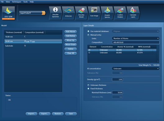
- The layered model for the sample needs to be described in the Set Up Solver step:

The figure above shows a layered model description for a sample consisting of a layer of Al2O3 on a substrate of Si and coated with a thin layer of C. The unknowns in this case are the thicknesses of the Al2O3 and C layers, and the exact composition of the Al2O3 layer.
Once the layered model has been described, press ‘Calculate Solubility’ and AZtec will calculate the best accelerating voltage (kV) to use for this particular problem, as shown below.
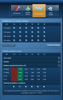
Once the solubility has been calculated, review the results, and set the SEM to use the suggested kV. For example, in the example shown above, it would be 10 kV.
5. Keep 'Described Model' values accurate/realistic
Specifically:
- The layer density (g/cm3). Very often when there are inaccuracies with LayerProbe results it is because the density is not correct. In fact, if you know the thickness of a certain layer you can use LayerProbe to interactively back-calculate the density.
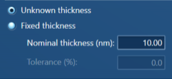
- Enter a nominal thickness (nm) for any layers in the model where the thickness is set as an unknown (as shown below). LayerProbe will start iterating from the nominal thickness to find a solution, so the closer the nominal value is to reality the more quickly LayerProbe will home in on a solution.

6. Perform a beam measurement
This should be done on the beam calibration standard (describe in point 3) before analysing the layered sample. To make this measurement navigate to Optimize > Calibrate:
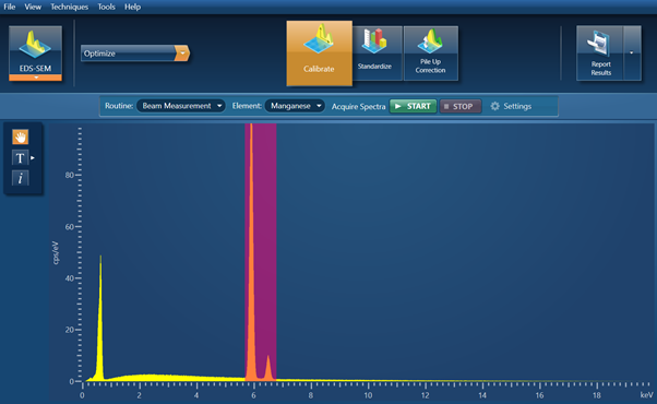
This Beam Measurement will be saved, will appear in the Data Tree, and will be used to produce the LayerProbe result. If the acquisition settings on the SEM are changed (e.g., kV, beam current) then a new beam measurement will need to be made before any further analysis of the layered sample is performed.
7. Collect an EDS spectrum as you would for quantitative EDS analysis
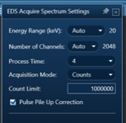
increase the SEM magnification to >1000x, use a process time of 4 or higher, turn the pulse pile-up correction on, and collect an EDS spectrum with a significant number of counts (e.g., 1,000,000) (see below). If this analysis is going to take too long, try increasing the beam current (keeping the deadtime below 50% for the selected process time). Remember if the beam current is changed a new beam calibration measurement will need to be made.
8. Compare Fitted and Theoretical spectrum
Once the EDS spectrum has been acquired move to the ‘Confirm Analysis’ step to review the LayerProbe result. Open the settings menu and check the boxes for both the Fitted and Theoretical spectrum to view them on the collected EDS spectrum (these spectra are pink and blue respectively). Along with the k-ratios, the goodness of fit between the fitted and the experimental (yellow) spectra, and the fitted and the theoretical spectra give an indication of the quality of the analysis and LayerProbe solution. If there is a significant mismatch between the spectra, and there are ‘% rel. diff.’ values in the table displayed in red, then try deselecting the affected X-rays lines and re-calculate the result by pressing the ‘Quantify’ button to see if the result is improved.
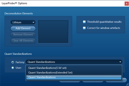
9. Select the appropriate standard set
Ensure that the appropriate standard set for the kV used is selected and used for the calculation of the LayerProbe result. For analysis conducted using an acceleration voltage of 5 kV or less use the ‘Quant Standardizations (5 kV set)’, and for 10 kV and over, use the ‘Quant Standardizations’ set (see below). Note, that slightly different element lines will be available with these two standardizations sets.

10. How to investigate spatial variations
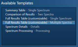
To investigate spatial variations across a layered sample collect multiple EDS spectra from across the sample surface (using Linescan if that option is available to you) and view them together by selecting the ‘Full Results Table (customizable) – Multiple Spectra’ from the list of Available Templates in the ‘Calculate Layers’ tab. Multiple spectra can be added to this data table by selecting multiple spectra from the Data Tree and pressing the ‘Add Selected Acquisitions’ button, which appears just below the Data Tree.
I hope that the tips and tricks detailed here help you to achieve high quality results on samples containing thin coatings, layers and films using AZtec LayerProbe.