In-situ heating experiments using EBSD are not a new thing. It has been done for many years, however, there is a growing interest mainly motivated by changes in manufacturing processes such as 3D printing. It is now regularly a consideration during the purchase of a new EBSD system, and in this situation, it is important to think of the whole system configuration and not just the effects of infrared radiation (IR) on individual detectors.
Some of the topics to consider are:
- Temperature requirements and associated emitted IR signal
- Equipment on the microscope, its suitability for analysis and potential risks of damage
- Mechanical implications or restrictions related to an in-situ stage
Effects of IR
High temperature EBSD experiments can be challenging due to the excess IR radiation that is emitted from the sample and the heating elements on the stage. Shielding on the stage has an influence, however, typically around 500-600°C, the intensity of the IR signal will cause a problem for the EBSD analysis. Initially, the IR will cause problems for background corrections but eventually, the intensity will result in the sensor being saturated and not able to acquire a useable diffraction pattern.
There are different solutions to this problem. The simple solution is to add a coating on the front of the phosphor screen to reduce the intensity of the IR signal getting to the sensor. This is a well-tested simple solution. However, it also reduces the intensity of the diffraction signal and, as such, reduces the sensitivity of the system. Practically this leads to a setup where either the user has to change phosphor screens regularly or the performance of the system at room temperature is compromised.
The image below provides an example of what happens inside the SEM chamber during a heating experiment and the effect on the EBSD signal.
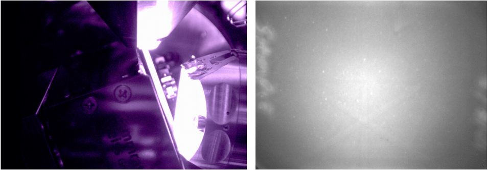
Left – Chamberscope image showing the high IR levels associated with the heating stage. Right – EBSD pattern collected from Si at high temperature, showing multiple artefacts associated with imperfections on Al coated phosphor screen.
A better solution is to only prevent the IR signal from getting to the sensor and thereby not compromise the sensitivity of the EBSD system. Besides performance benefits, it also makes the system easier to use, as it doesn’t lead to changes in the background signal due to IR. The implementation of this solution is not identical for all EBSD detectors, nor is it offered for all detector designs, however. Years ago, an interference filter solution was implemented for the lens-based Nordlys detector range, and it has been used by many customers, giving us positive experiences with this approach. Recently, a similar solution was launched for our CMOS EBSD detectors which now makes it possible to use the higher sensitivity and speed of the Symmetry S3 in combination with heating experiments.
The data acquisition speed is important, as the reason for doing the experiments is to gain knowledge by observing microstructure changes as they happen and not be limited to individual snapshots. The graphics below provide an example of data which can be obtained by combining EBSD and in-situ
heating.
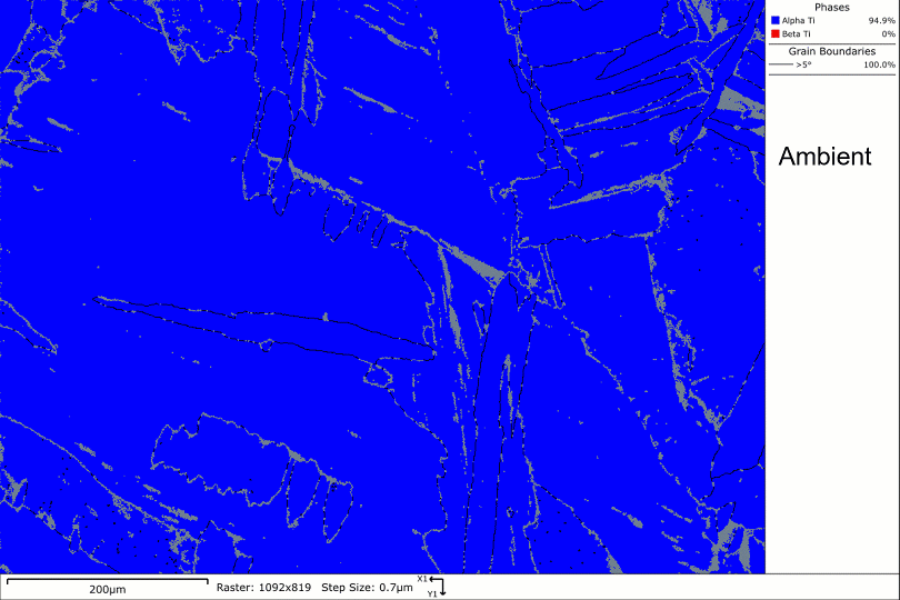
Series of phase maps collected during a high temperature EBSD experiment on a Ti sample, showing the phase transformation from α (blue) to β Ti (red). Note that the temperature shown is the heater temperature: the actual sample temperature is estimated to be ca. 50 °C lower.
Suitability
EBSD detectors are normally designed so that the phosphor screen can be replaced easily. This is because it is the most likely part of the detector to get damaged and replacement screens are typically offered as consumables.
This is also important in relation to high temperature experiments, as there is an increased risk of damage to the screen which means that screen and potential FSD diodes should be considered as replaceable parts.
The Symmetry S3 detector was designed with field replacement of phosphor screen and diodes in mind, making it possible to exchange or remove parts when needed.
The EBSD detector is typically not the only detector installed on the SEM. It is important to consider risks to all detectors on the system and not just focus on the detectors which are expected to be used during the experiments, even though they are probably the detectors at highest risk.
Calibrations and Mechanics
There are many different designs of heating stages or setups, depending on the experimental requirements. Some involve a minor module mounted onto the normal SEM stage; others basically replace the normal SEM stage with a dedicated experimental stage.
In some cases, the analysis conditions (working distance and tilt) will be different from standard room temperature analysis because of the space requirements of the in-situ stage. This is important to consider, as it can have an impact on the performance of the EBSD system. The Symmetry S3 detector has elevation controls which makes it possible for the user to optimise the position of the detector relative to the sample. This functionality has many benefits in relation to large samples or Large Area Mapping. However it is also important in relation to in-situ setups, as it means that the geometry can be optimised both for the in-situ and room temperature analysis, even if under different microscope conditions and geometry.
Looking forward
Current customer requirements are driving developments towards integrated solutions. This means not just having the technical capability to combine analytics like EBSD and EDS with in-situ
experiments but also being able to automate the experiments and data acquisition.
This will be discussed in a coming webinar and blogs.


