Site specific lift-out is a frequently used method for preparation of TEM lamella samples in FIB SEM, and similar workflows are also used for a range of other FIB applications including 3D and cross section analysis. Analytics, such as EDS and EBSD, are often used at the start of this process to locate the site of interest or toward the end, for analysis of the final prepared sample.

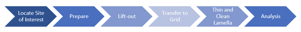
Figure 1 - Typical lift-out workflow
While we traditionally think of a nanomanipulator as only being used during the ‘Lift-out’ and ‘Transfer to Grid’ steps, in some cases an OmniProbe nanomanipulator can also be used to help locate the site of the interest or be used during the preparation step.
Locating Site of Interest
An OmniProbe nanomanipulator can supplement the imaging capabilities of the FIB SEM by using tip biasing in combination with either SE or BSE detectors to provide voltage contrast imaging, a method which can help identify failures in integrated circuits or defects in materials. For voltage contrast imaging the sample is observed using different surface potentials (delivered by the probe tip) and the effect on the signal is monitored.
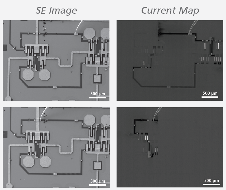
A more advanced option is to use the nanomanipulator as an electrical contact made to a specific point on the sample and measure a response signal such as EBIC (electron beam induced current) or EBAC (electron beam absorbed current) which is generated by scanning the electron beam over the sample surface. Depending on the sample this can show defects in materials such as solar cells (there is an application note on this here), or failures in electronic devices as illustrated in Figure 2.

Figure 2 - Microchip with an open circuit which is observed as a break in the conductive path. SE images and measured current maps acquired with the probe making contact to two points on the sample, showing different parts of the connected path on the current maps.
Preparation
The preparation step prior to lift-out typically involves a localized deposition of a protective layer (such as Pt) using a gas injection system, followed by cuts into the material using the ion beam.
On conductive samples this is straightforward, and examples have been given in blogs by one of my colleagues. Non-conductive samples, or features such as insulating layers and inclusions, can however present challenges both for the deposition of the protective layer and the following milling because charging causes the beam to be deflected, disrupting the scanning pattern.
In this case one option is to use the OmniProbe manipulator to provide a local grounding point on the sample, helping to stabilize the electron and ion beams of the FIB during the Pt deposition process and the following milling. This can be done through the OmniProbe software, where the operator can control whether the probe tip is to be grounded, biased, or used to detect an electrical contact.
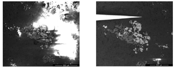
Figure 3 shows an example of the OmniProbe being used to provide electrical grounding and by doing so making it easy to image the nearby non-conductive features on the sample. The same grounding strategy can also be used in combination with EDS analysis of non-conductive samples for applications where carbon coating the sample might not be a suitable solution. Without mitigating charging during EDS analysis results can be misinterpreted due to local changes in the effective beam energy which effect the generated x-ray signal.

Figure 3 - Non-conductive sample imaged using electron beam. On the image to the right, the OmniProbe has been used to provide local grounding.
Conclusion
An OmniProbe manipulator is most frequently used for lift-out and transfer of samples to a grid, but it can also be used to assist the whole lamella preparation workflow. This includes using the probe to identify features of interest which need to be targeted for lift-out and providing local grounding to stabilise imaging of non-conductive samples.