Transmission Kikuchi Diffraction (TKD) is an Electron Backscatter Diffraction technique that is capable of characterising phase and orientation information for nano-structured materials. Keller and Geiss[1] obtained the first data over a decade ago. Since then, the technique has evolved and become commonly used as a solution for improving spatial resolution when the limits of conventional EBSD are reached.
TKD analysis is done using an electron transparent sample. The diffraction signal is generated from the lower side of the sample, resulting in a different setup compared to conventional EBSD. The early TKD work was done using conventional EBSD hardware and software, which required improvements of band detection and indexing routines to deal with distortions and broader bands in the diffraction pattern.
Why does sensitivity matter?
To improve spatial resolution and data quality, there are several issues to consider. These range from sample preparation and cleanliness to the setup and use of the SEM and EBSD/TKD system. When acquiring data at high magnification, it is important that the system is stable, as minor instabilities can lead to drift. Sample cleanliness is more critical, as we need to avoid contamination build up which otherwise can lead to poor data quality. To get the best performance of the electron column for this application, we typically want to work at a short working distance (close to the pole piece), high beam energy (to reduce spread of the transmitted beam) and low probe current (to reduce the spot size of the beam).
Balancing all these parameters can be challenging, but essentially, we need to work at reduced probe currents to get the spatial resolution while acquiring the data as fast as possible to reduce instability issues, which otherwise leads to contamination and drift. This means that the detector needs to be as sensitive as possible, so that we efficiently collect the signal generated from the sample, enabling the use of low probe currents or short acquisition times (high speed).
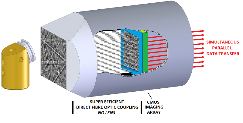
The Symmetry EBSD detector was developed with this in mind and is today still the most sensitive detector due to its unique fibreoptics design, which allows us to collect high quality EBSD maps for a wide range of applications.

Figure 1: Unique optics solution for Symmetry S3 providing high sensitivity for EBSD analysis.
Does the geometry matter for TKD?
The early work done by Keller and Geiss used regular EBSD hardware, and a geometry setup was developed based on this requirement; the setup often referred to as off-axis TKD.
Intuitively, if the detector screen is brought closer to the sample, we can collect more signal, and if the screen is angled, then we can reduce band width variations across the collected pattern. However, if the primary beam hits the screen, then besides X-rays, it can lead to damage. Also, the high intensity signal will saturate the sensor, resulting in a part of the screen being unusable for collection of a diffraction pattern.
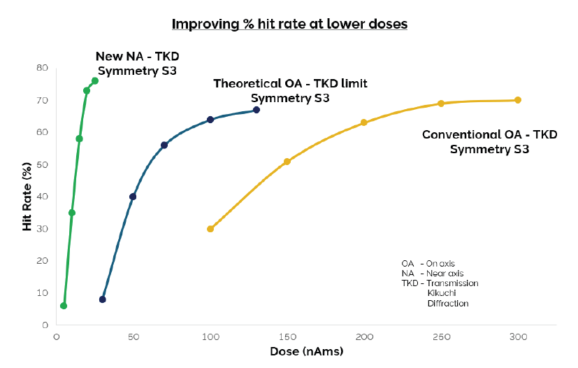
Analysing the effectiveness of different geometries on a range of samples showed that, by changing the setup, we can improve the sensitivity of TKD analysis by an order of magnitude.
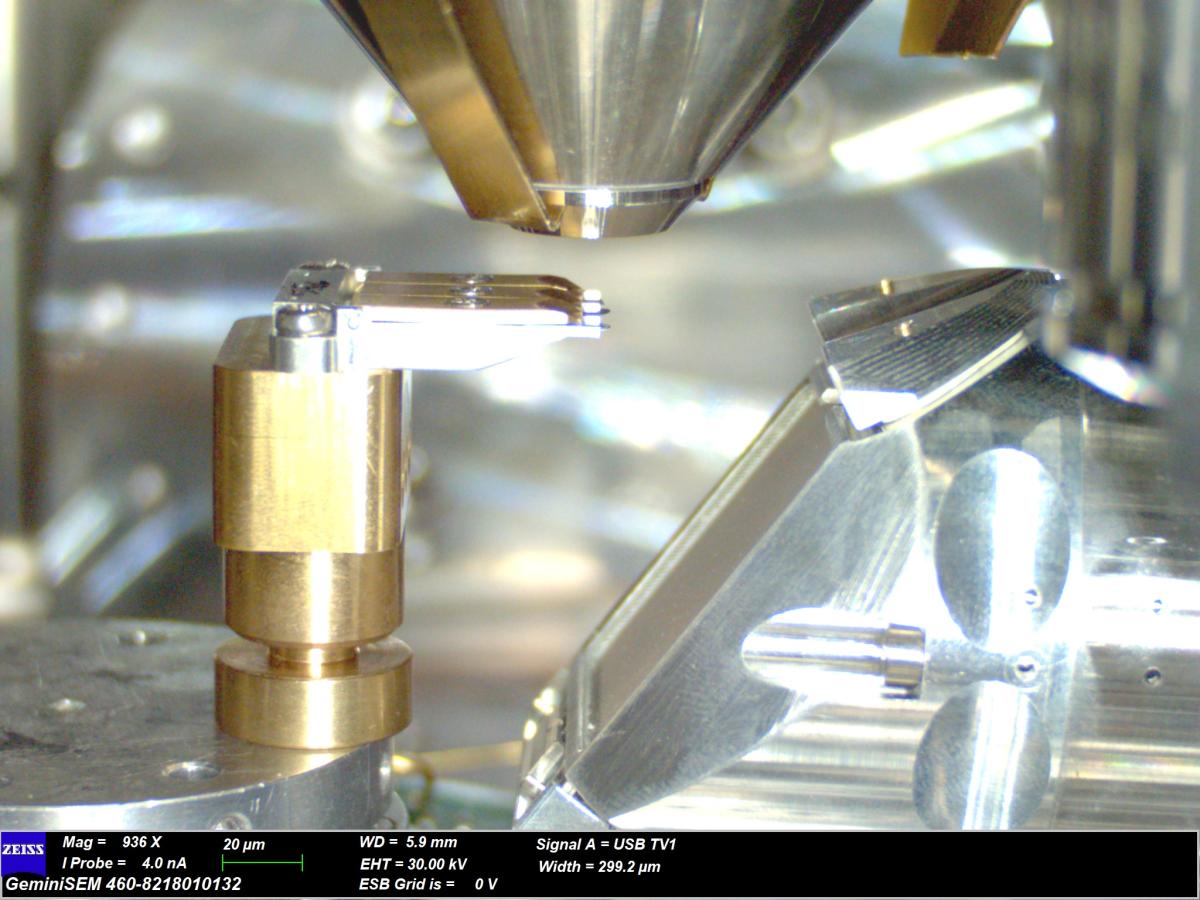
Figure 2: Left hand side showing setup for NA-TKD. Right hand side showing performance curves for different TKD geometries.
Applications
Next step was to use the Symmetry S3 detector with the newly developed screen in a Near-Axis TKD setup (NA-TKD) in comparison to conventional setups to verify the results from the development process.
Several samples showed that it was now easier to work with lower probe currents and thereby improve the spatial resolution – even on samples which were not in the best condition. The improved sensitivity also means that analysis of beam sensitivity samples becomes possible.
Hopefully, we will soon be able to share some of the data as application notes, so keep an eye on our website for more information.

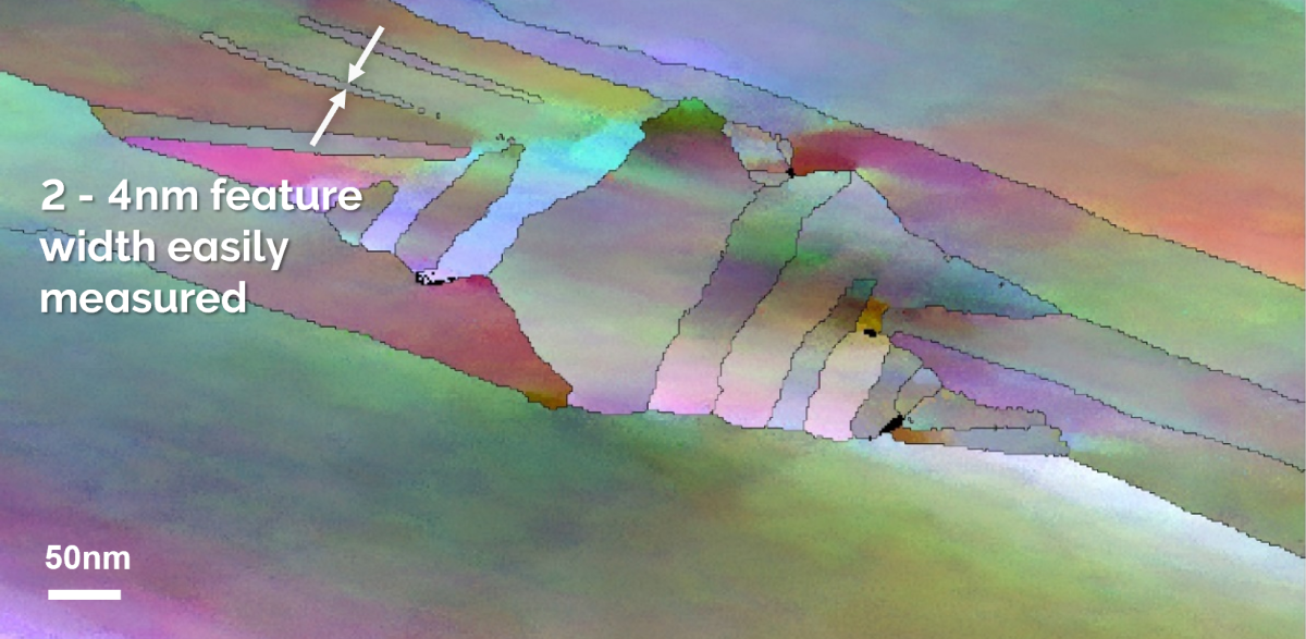
Figure 3: Example TKD map from steel sample showing resolved nanoscale features (twins).
NA-TKD tutorial coming soon
While the developed solution is compatible with all our CMOS detectors, it works best with the Symmetry S3 detector. There are several considerations related to working with this setup. If you are interested in learning more, then join our tutorial in September.