7th April 2021 | Author: Kim Larsen
Globally, there are a lot of projects related to climate change and how to make better use of green energy. One of the big targets is to improve solar cell materials and make the use of solar panels more common, thereby reducing CO2 emission.
In solar cell materials, defects and impurities can have a huge impact on the final product, acting as recombination centres for charge carriers. The main defects in multicrystalline Si (mc-Si) affecting performance are point defects (e.g. particulate impurities), linear defects (dislocations) and planar defects (e.g. grain boundaries).
Where does Oxford Instruments come in?
At Oxford Instruments, we normally work with well-established SEM and FIB based analysis techniques, and so finding solutions to new developing applications provides an interesting challenge. EDS can be used to quickly identify based on chemistry. This can be used to avoid contamination of the production material and thereby prevent certain defects from being created in the first place. However, it is more difficult to quickly characterise boundaries or dislocation defects.
Traditionally, defects in mc-Si have been investigated using photoluminescence and electroluminescence imaging techniques. Neither of these provides a resolution on the nanometre scale, however. Therefore, neither is suitable for identifying and characterising small defects such as dislocations.
Developing a working method
On the FIB, we are used to working with nanomanipulators which can be accurately positioned and used to make contact to the sample at specific points. If the nanomanipulator has suitable electrical connections, then the tip can be used as an electrical contact point and electronics can measure the current flowing through the probe as the electron beam is scanned over the sample. This generates an image showing variations in the induced current and thereby provides a method for imaging defects on the nanometre scale.
Being able to use the same equipment and setup for a wider range of analyses gives a faster and more secure workflow. The risks associated with handling of samples during transfer is significantly reduced, and the use of the high precision OmniProbe provides a single solution for EBIC and liftout. With electrical measurements in FIB becoming a more established analysis method it seems likely that we will be seeing many other applications being developed.
Our solution in practice
EBIC (electron beam induced current) compatible nanomanipulators can be used both as electrical contact for EBIC imaging and for lift-out of samples when used on a FIB. The setup looks as shown in figure 1. The OmniProbe is used as electrical contact while the sample backside is grounded via the SEM stage. An alternative method for ensuring good ground connection would be to use the EBIC sample holder, which we have recently developed.
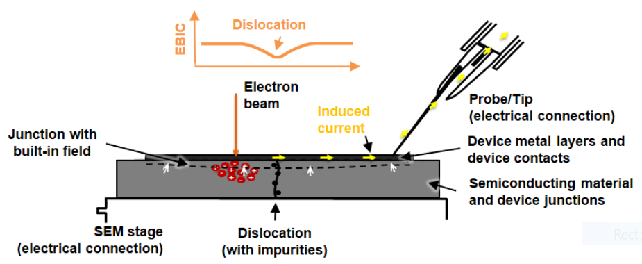
Figure 1 - Schematic showing EBIC signal generation in solar cell material and measurement using OmniProbe manipulator
A p-type mc-Si was etched in order to reveal the defects in the material. It was then loaded into the FIB using a similar setup as shown on the schematic in figure 1.
Figure 2 shows how the defects can be imaged, covering a wide range of length scales from mm to nm. By using the OmniProbe in this way, it is easy to first identify the location of the defects and then prepare TEM lift-out samples containing the defect to allow further characterisation without having to use additional equipment. Figure 3 shows the defect as a white spot in the lamellae which has been attached to the TEM half-grid.
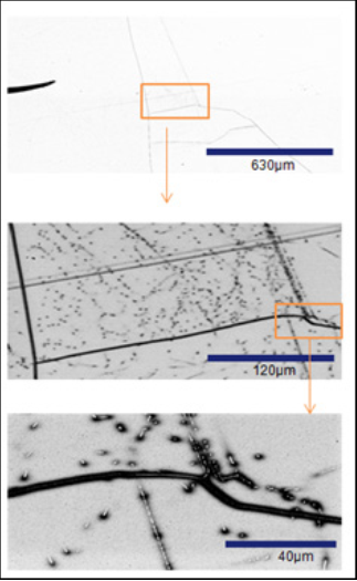
Figure 2 - EBIC imaging of defects and grain boundaries across multiple length scales.
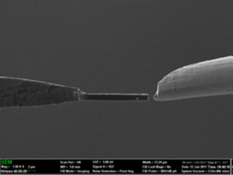
Figure 3 - Liftout sample containing defect (white spot) in the lamella.
Developing a consistent method for identifying defects in solar cell materials is essential to improving quality on a commercial scale. This blog post details the solution that Oxford Instruments has developed to identify and characterise these defects and dislocations. If you’re interested in learning more about this solution, please download our recent application note which details the process in depth.


