Since joining Oxford Instruments, I have been embarking on a mission to highlight the potential that Raman spectroscopy can offer the SEM community. It is seemingly a technique that many have heard of but never really used and I am trying to change that. The RISE (Raman Imaging Scanning Electron) system is the perfect tool for this job as it bridges the gap between optical and electron microscopy.
In several of my previous blogs, I’ve explored the principles of Raman spectroscopy and where it fits in the world of material analysis. I have also presented a recent tutorial which explores the RISE product in more detail. If you missed this then don’t worry, we have brought it back for a second time, the details of which can be found here.
To quickly summarise, RISE offers users the opportunity to generate images based on the molecular fingerprint of the material at that specific point, adding an additional perspective to the conventional SEM analytics, such as EDS (Energy Dispersive Spectroscopy).
In this blog, I provide a methodical approach to conducting RISE measurement. I will also discuss the important aspects that should be considered to make sure that we get the most out of your analysis.
Is the sample compatible with Raman spectroscopy?
The first thing we need to do is make sure our sample can be analysed with Raman spectroscopy. A good rule to remember is that Raman scatter can be obtained from everything except metals and simple salts, so as long as the sample doesn’t fall into one of these categories, then it should be fine. Another very important consideration about the sample is whether it has been coated for Scanning Electron Microscopy (SEM). I know that this if often preferred but for RISE, samples should remain uncoated so that the laser can interact with the material. If your sample satisfies both these conditions, then it is likely that Raman information can be obtained.
Focusing on the point of interest
A fundamental step of any microscopy technique is focusing the sample, and the RISE system is exactly the same but with an added twist.
Firstly, the point of interest (POI) should be identified using SEM imaging, and it is very important to be careful with beam parameters here. Exposing the sample to the electron beam can lead to carbon deposition which negatively affects both the EDS and the Raman spectrum. My colleague, Dr Sam Marks recently addressed this problem in another blog.
Once the POI has been found and brought into focus, the stage movement to the RISE position can take place.
Now something I am personally excited about is incorporating the speed and performance of the new Unity
BEX detector into this part of the workflow. The combination of both backscattered electron and X-ray images will mean rapid identification of features, so we can be faster at targeting the RISE analysis.
Back to the topic at hand, the RISE instrument is essentially a confocal optical microscope within the SEM chamber, and when we move to this position, our same area of interest will be in the field of view. However, a small amount of focusing might be required.
Here comes that twist I mentioned; or confocal Raman microscopy, we need to ensure that the laser is focused on the sample. To do this, we use the Oscilloscope tool in WITec’s Control software, which provides a continuous spectral readout from our surface. Adjusting in the Z-axis will move the confocal window, and when we see the most spectral counts from the surface, then we know that our laser is in focus.
Our RISE experiment
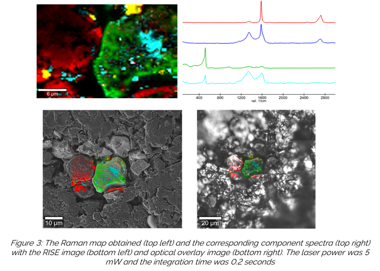
The control software is the brains behind our RISE system in a similar way in which AZtec is to our EDS detectors. It comes equipped with a range of measurement tools which help to drive the Raman analysis. We can generate single point Raman spectra, giving us the molecular information of any given point. There is also a linescan tool, which means we can see how the Raman information changes between 2 points. Most importantly, there is the large area scanning tool which is what produces the detailed hyperspectral Raman maps. All these tools come with the adjustable parameters, allowing users to design their experiments to the desired specifications.
As is customary with any experiment, there are variables that should be considered before the analysis is set in motion. Specifically, we need to define the dimensions and resolution of our Raman map. This is similar to what we do before we run an EDS map, but we need to remember that we are unfortunately limited by the laws of physics. The spatial resolution with the RISE system is less than 400 nm. This is useful to know, because we can use this information to make sure the mapping parameters are optimised. Raman imaging scans the sample point-by-point and line-by-line, which we can correlate with our scan geometry. For example, let’s say the area of analysis is 100 µm by 100 µm, and we want the Raman image to have an optimised resolution. To do this, our points value would be 300 and our lines value to be 300. This would be equivalent to just over 3 pixels per 1 µm (and remember our spatial resolution is 400 nm) which means this is at the very limit of our spatial resolution.
The power of the laser is a very important factor to consider. We like to say that Raman microscopy is non-destructive, however this is not strictly the case. What we are doing is concentrating our laser light into a very focused point, much like when we hold a magnifying glass into the sunlight. Therefore, if our laser power is too high for a specific sample, then it can become very destructive, very easily. Care must therefore be taken unless you are desperate to burn a hole in what could be a very precious sample.
Another variable is our integration time. This is the time where we are collecting our Raman scattered photons. The longer the integration time, the more time the sample is irradiated by our laser at that specific point. This can be beneficial, if the aim is to obtain a highly resolved Raman spectrum, but can lead once again to sample damage. In the case of point analysis, it is about finding balance between the integration time and the number of accumulations. For Raman mapping, integration time is also important, as it defines the information contained within that single pixel. If it is too fast, then we might obtain too little spectral information.
It is important to note that the wavelength of the laser light is also very important. Typically, a 532 nm laser will be suitable for most samples, because it offers a nice balance. 532 nm is at high enough energy to excite the molecule and at a high enough wavelength therefore not inducing fluorescence. In the rare cases that this 532 nm laser is not suitable, then we can simply equip a different wavelength that will be more suitable.
Once all these parameters have been configured, we can run the scan and generate the RISE image, giving us the final result…
RISE and Raman spectroscopy may still be relatively new to a lot of readers, but I hope you can start to see the potential that such a technique can offer. The incorporation of Raman microscopy to the SEM chamber means we can seamlessly correlate information on both the atoms and bonds of the material. Hopefully, this blog provides a good picture of the steps taken when designing the RISE map but also the key parameters to consider so that you get the best result.


