I have met many new users of EBSD in recent years. The obligatory first question they ask is “what SEM settings should I be using”? Beyond the obvious accelerating voltage and beam current settings, the next big (and much simpler) question is “what magnification should I use”? My response requires an additional question; “what are you trying to do?” The common response is either texture and/or grain size analyses. The texture response is usually simple; typically, a low-mag, high speed approach will give the statistics that make for good texture analysis. But what about grain size analysis. How do we determine the appropriate field width, and subsequently, the proper step size to get good results?
Turning on the light
The proper magnification for grain analysis is revealed in the imaging step, but it’s often not as simple as just examining the SE or BSE image on the SEM itself. I liken using the SEM to find an area of interest to walking around your house in the dark. There is always a chance you will find what you are looking for, but no one wants to walk into a wall or trip over something in the process. Turn on the lights! Get more information on where you are going. AZtec provides some key tools to make things easier. However, I notice many users overlook an inconspicuous but valuable tool, “Continuous Scan”.
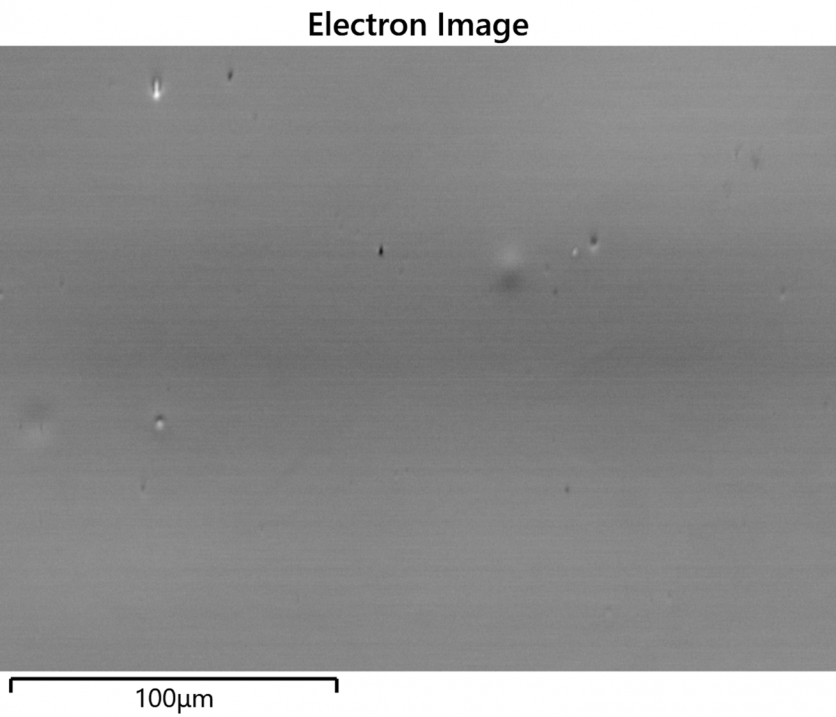
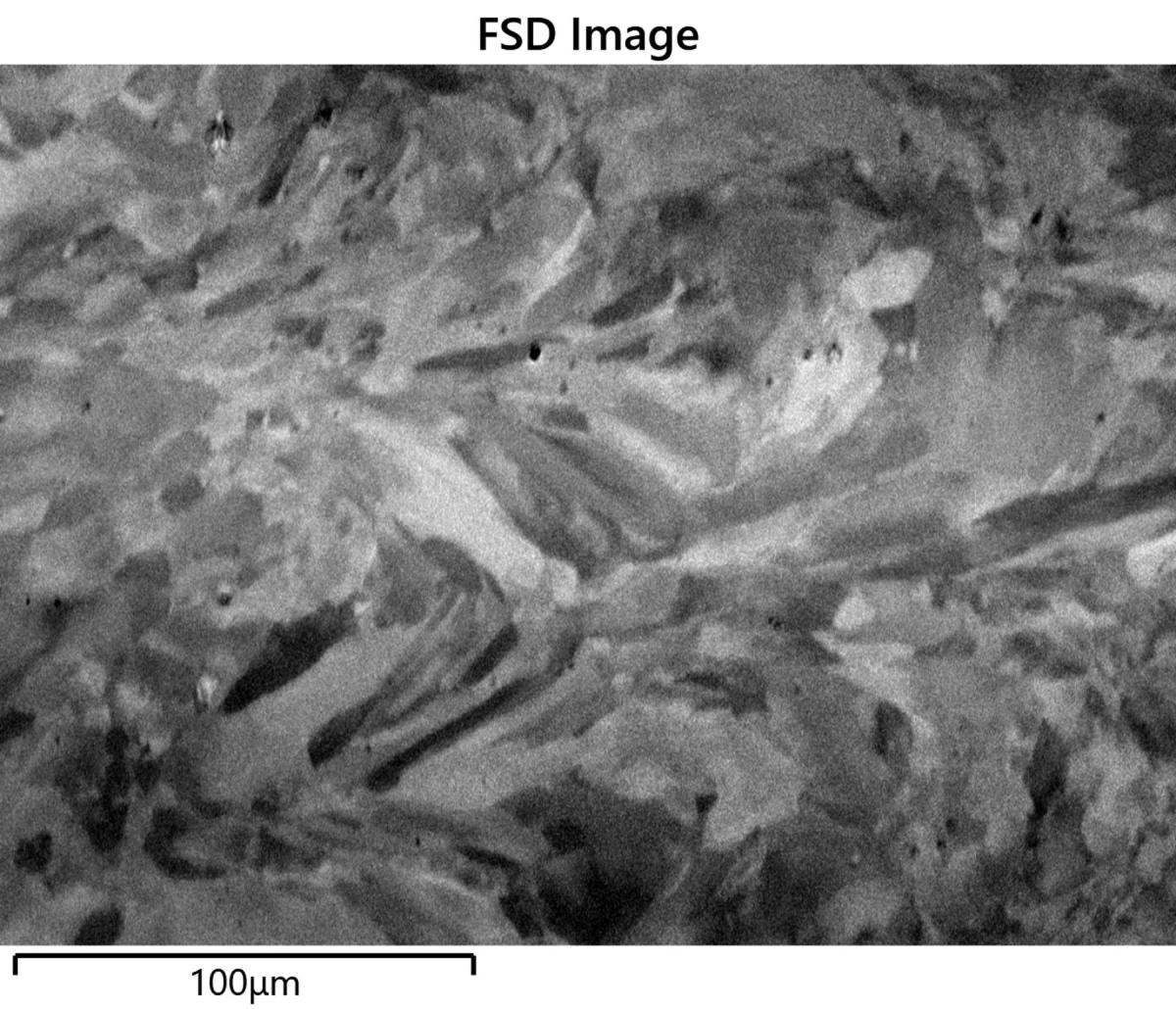
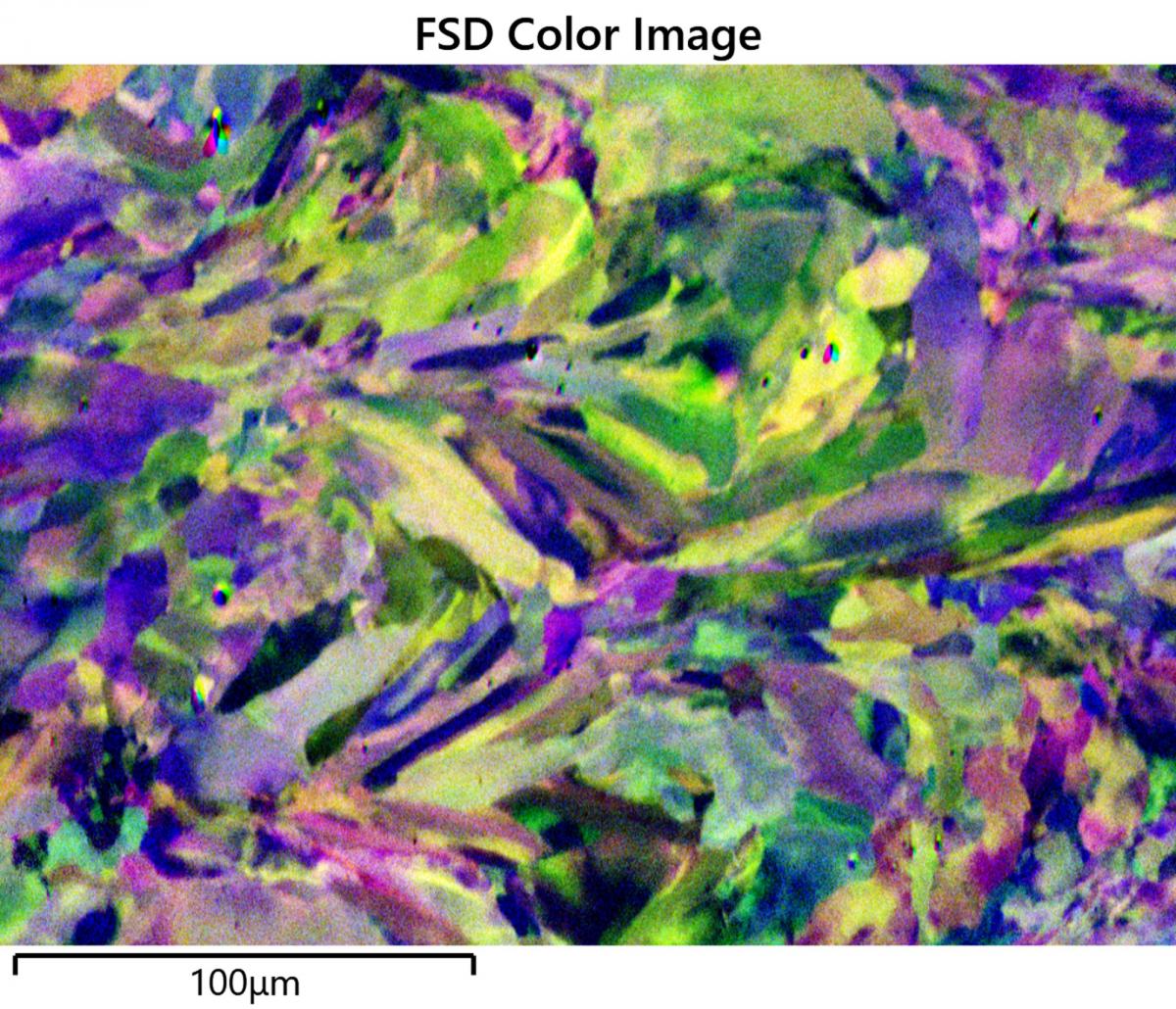
Every imaging step has a Continuous Scan option - the green infinity button to the right of the settings on every Scan Image step. Since EDS does not have an additional imaging source, most users tend to overlook the tool. Our CMOS detectors have the option of 5 forescatter detectors (FSD) that offer considerably more information than the detectors on the SEM. Figure 1 shows just this effect.
Figure 1: Additive stainless steel sample. The electron image on the SEM (a) only revealed that the electropolishing was good. The unique grain structure was revealed by the FSD Image (b) and (c) – coloured.
Polished performance
With EBSD, having a well-polished, flat sample is critical to the success of the analysis. The flipside is not having any discernable features in the sample makes focusing difficult. Using FSD reveals the grain structure allowing proper focusing and better assessment of the appropriate field of view needed. Combining this with continuous scan allows for a true targeted search and not a hunt-and-peck method that can be time consuming and unproductive.
The three lower FSDs are especially valuable to the grain analysis setup. In transmission Kikuchi diffraction (TKD) the diodes reveal the same information as a STEM darkfield detector would. More recently, AZtec has added the ability to change the polarity of one of the three diodes to create an oriented darkfield mode. In traditional EBSD at 70° tilt, the same diodes provide details on topography and orientation. AZtec allows the individual diodes to be colour-coded to further enhance the grain visualization.
With the detector fully inserted, topographic effects can dominate the contrast of the image. This often emphasizes contaminates (which can be great for focusing) and can reveal imperfections in sample preparation. All these can mask the orientation contrast that is truly sought after. Retracting the detector a few millimetres can shine a light on relative orientation and grain size and improve the colourisation effect. Figure 2 shows the improved orientation contrast between a fully inserted detector vs one retracted 8 mm. The colour image goes from low value to something that discerns grains and those with similar orientation without even collecting a diffraction pattern.
Figure 2: Duplex stainless steel. The upper row is captured at the fully-inserted position of the EBSD detector and reveals more topography effects. There’s more contrast but the colour image is muddled. The lower row is captured with the detector retracted 8mm and shows fewer topography artifacts. The image is based purely on orientation differences and makes a very good colour image.
Once an area of interest is found and a good electron image is obtained, an appropriate step size for mapping must be determined. One needs to consider the ultimate goal of the grain analysis at this point. If morphology data is the dominant concern, then a larger step size can be used. Point-to-point data within the same grain will be less valuable to this application so fewer points are used to save time. The rule of thumb is, use a step size 1/10th the average grain size to achieve a good representation of grain morphology. The grain analysis settings in AZtecCrystal reflect this generality, using 10 pixels/grain as the default minimum value for detection. There are certainly exceptions to the rule, most notably when doing intragranular measurements where a smaller step size is required. Readers interested in more information on grain detection within AZtec and AZtecCrystal should watch the video “Measuring Grain Size using EBSD” by Dr. Pat Trimby.
Key take-home
The key takeaway to this blog is please do not feel like there is guesswork in your EBSD setup. Unique to EBSD among other microanalysis techniques is imaging available within the detector itself. It can be run in real time, and the position of the detector can be changed to shed light on your sample before you even begin to set up the camera settings. Do not feel limited to the SEM imaging as more information is available within AZtec.
Michael Hjelmstad,
Applications Specialist, Oxford Instruments