Personally, I would say most electron microscope users are familiar with Energy Dispersive X-ray Spectroscopy (EDS), the widely accepted and routine technique for determining the elemental composition of materials. During the interaction of electron beam with the sample, one of the emitted signals that can be analysed is X-ray. These characteristic energies/wavelengths and can be detected using either a solid state energy dispersive detector (EDS), or with a diffracting crystal in tandem with a proportional counter used in wavelength dispersive spectroscopy (WDS). Both techniques have their merits.

EDS (yellow) and WDS (grey) spectra from the same material, the 10x better resolution for WDS clearly shows even the most closely spaced X-ray peaks for analysing complex samples or detecting minor or trace elements.
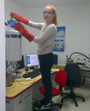
My analytical journey started with using EDS. Please ignore the health & safety violations in this photo, but what you can notice is that I am pouring liquid nitrogen to use an old style LN2 cooled Si(Li) EDS detector, shown in Figure 1.
Figure 1: Where it all started: filling up an old style Si(Li) EDS detector.
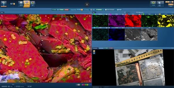
What is great about the EDS technique is that it can work in a “point and press” manner. You can quickly check the constituent elements and composition of your sample without any prior knowledge. Since we moved over to SDD detectors which allowed us exceptional throughput, we can now rely on Live Chemical Imaging (LCI) to see real-time imaging and chemical information while moving around the sample. In the past year, we have also seen the introduction of the BEX (Backscatter Electron + X-ray) imaging technique for even faster and more vibrant live imaging of a sample (an example is shown in the screenshot of a BEX investigation in Figure 2). This is a massive jump from what was possible with the slow acquisition of Si(Li) detectors, with which I started my journey into microanalysis world.


Figure 2: Where are we know: Screenshot of BEX imaging using the Unity detector to study Augite diabase sample. Image (left) reveals morphology and sample chemistry in high definition in real time.
Before I have started my PhD at University of Strathclyde, Glasgow, I was familiar with the term Wavelength dispersive spectroscopy (WDS), but I didn’t have any practical experience with the technique. So, for those of you less familiar with this term, what is WDS?
WDS is a technique complementary to EDS for performing X-ray analysis of materials. The goal is the same as with EDS, to determine elemental composition of the sample, and it is used for the same purpose; so you might ask yourself, do we then need WDS?
Well, the answer is yes; in certain cases, you need a much higher confidence degree of in the identification of the elements detected with the EDS, or you need to measure really low concentrations of elements that are below the detection limits of EDS. This will lead us to need a different, higher specification tool.
For example, why did I need WDS for my PhD? Well, for similar reasons. I was analysing different compound semiconductor materials, particular AlGaN and GaN materials. Among the things I was interested in were the effects of n- and p-type doping and AlN content on the quality of the materials. So, I needed a technique that could provide accurate and precise compositional data as well as the possibility to measure low dopant concentration. The WDS technique came to the rescue and a new area of my analytical journey could begin.
Now, let’s move away from my personal experience, and I will highlight some of the most common examples where you might benefit from WDS.
1) Separating EDS peak overlaps
If we compare EDS (yellow spectrum) to WDS (grey spectrum) in thisvideo, we can see that we can separate S and Mo X-ray peaks in the WDS spectrum while we simply cannot do that based on EDS data (Figure 3). Ultimately, we can more confidently measure these elements using WDS. With WDS, it is straightforward to identify the elements present, and then we can also quantify their abundance without resorting to a deconvolution procedure.
Because WDS provides a higher energy resolution, typically 10x better than EDS, adjacent spectral lines which cannot be observed separately by EDS can now be detected separately. WDS resolution also does not degrade at higher count rates. If you are interested in numbers, EDS energy resolution varies between about 50-250 eV, while WDS is 3-30 eV typically.
In the video, you will notice the complex mechanical requirements of WDS design, which is quite unlike EDS. This requires state of the art engineering and craftmanship. All our WDS spectrometers are custom built in our factory in UK and thoroughly tested to achieve this best performance.
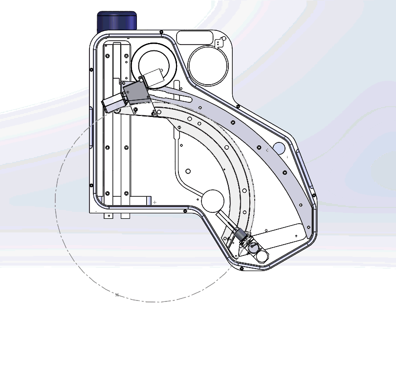
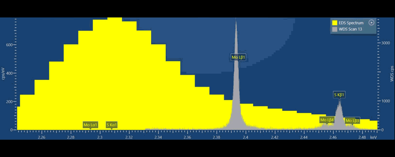
Figure 3: Graphical video showing what is happening inside a WDS spectrometer when we acquire a WDS spectrum: the analysing crystals and the X-ray detectors are mechanically moved along the circumference of the Rowland circle in order to independently detect the characteristic X-rays of each element. The second video shows the production of a WDS scan over the S and Mo X-ray peaks and the difference between the EDS spectrum in yellow and WDS spectrum in grey.
What are other benefits of the technique?
2) Trace element identification and mapping
Let’s start from the minimum detection limit, essentially the smallest concentration of an element that can be detected by a technique. Quite often, it is defined as a peak height equal to three times the standard deviation of the background counts. For routine EDS analysis, the detection limits are at best about 1000 ppm or 0.1 wt%.
From the video, you may have noticed there is a big difference in peak to background ratio (P/B), between WDS and EDS. In the WDS scan, the background intensity is significantly lower than the EDS which aids in the discovery of very small intensity peaks.
As the peak to background ratio is significantly improved, so WDS can detect trace elements of 100 ppm or sometimes considerably less, resulting in the detection of trace elements using WDS being up to two orders of magnitude better than when using EDS.
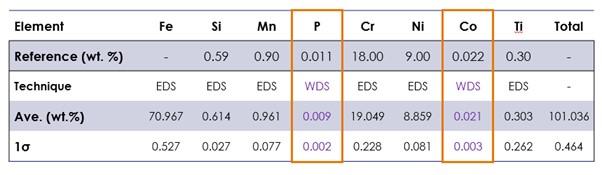
For example, a steel analysis can benefit from the improved P/B ratio with the characterisation of low levels of P and Co (Figure 4).
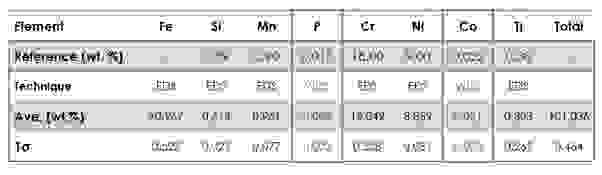
Figure 4. Quantitative combined EDS-WDS results on steel sample (average of 6 points), highlighted results for trace elements.
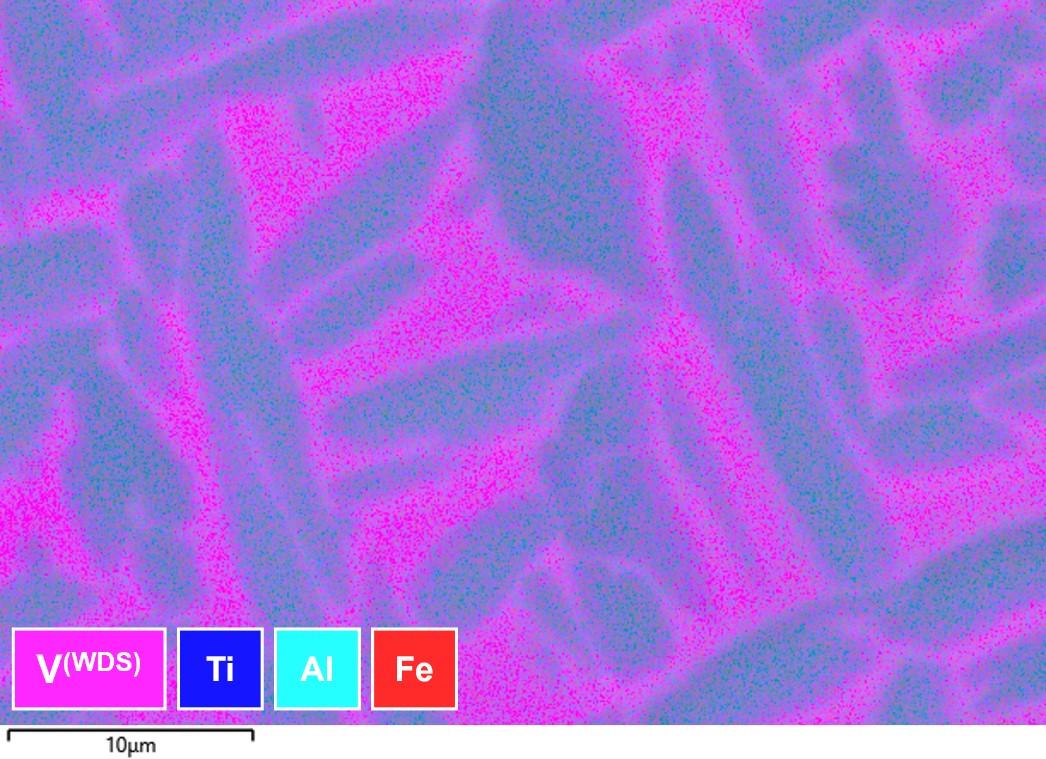
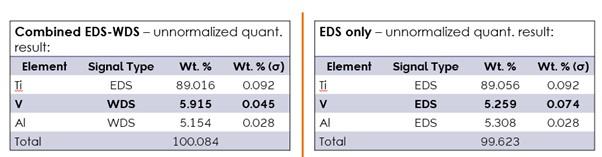
We don’t have to stop with quantitative analysis. We can also map trace/overlapping elements, as in the example shown in Figure 5, where WDS is used to map alloy segregation. In this case, we are using WDS to characterise the V which is part of a severe overlap with Ti (the dominant element in this alloy) in the EDS spectrum. More on this below and in the link
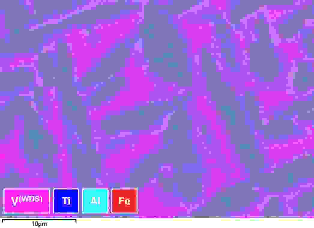
Figure 5: Map showing Ti, V and Al distribution, using a combination of WDS and EDS simultaneously acquired to analyse alloy segregation.
3) Accurate and precise quantitative analysis, with lower errors
WDS provides high quantitative accuracy and precision which is comparable to that of wet chemical analysis. WDS quantitative analysis requires measurement of a standard sample and doesn’t use the standardless quantitative analysis techniques (built-in standard database) used in EDS. The example in Figure 6 highlights much lower uncertainty and improved accuracy on the V measurements obtained via WDS in the Ti alloy sample.
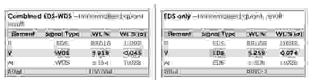
Figure 6: Ti alloy sample analysis, V measured with WDS vs EDS
4) Increased sensitivity to light elements
One problem with light elements measurements (Z<11, Be-F) is that relatively few X-rays are emitted during excitation, and these low-energy photons are easily absorbed by the sample. In the end, low count rates will result in lower precision. In addition, peak to background ratios are particularly low for low energy X-rays making the higher performance of WDS particularly important, especially when levels are low. WDS uses special multi-layered crystals for this purpose, as they maximise scattering efficiency to pick up the wavelengths produced by the light elements.
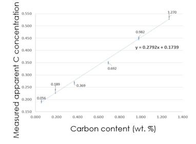
For example, we can measure low concentrations of boron and carbon in boride and carbide inclusions or trace levels of light elements, such as boron, carbon, and nitrogen, in a metal matrix. Figure 7 shows how we can use WDS to produce a calibration curve of C content, which greatly improves the accuracy of measured C content in unknown steel samples.
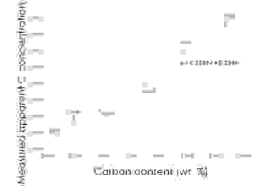
Figure 7: A calibration curve for the analysis of C in steel by measuring a set of standards with C contents ranging from 0.056 to 1.27 wt% using WDS.
So overall, we can say that with WDS, we can overcome some of the limitations of EDS. We can achieve much higher energy resolution, so that closely spaced peaks can be easily separated, and we can achieve much lower background levels, so that detection limits are greatly improved. And we mustn’t forget another important conclusion; that the end result of using WDS is that you have much higher confidence in the identification of the elements detected in any analysis, and you can gain the needed confidence to get to the correct interpretation of the results.
If you remember, at the beginning, I did say that EDS is often used as a “point and press” method while WDS cannot be used in that way. With WDS, we measure X-rays separately for each wavelength so multiple elements cannot be analysed simultaneously (unlike EDS) and accordingly WDS requires a longer measurement time.
While this has potential to be a big drawback, there is also a solution to this issue. In our AZtec software platform, WDS analysis is fully integrated with EDS. Therefore, we can bring together the advantages of both techniques – speed and sensitivity. EDS can be used for initial screening and for the analysis of major elements (i.e. those unaffected by peak overlaps), while WDS can be used in more challenging examples. This saves on measurement time and maximises the accuracy and precision of the measurement of every element. We have even incorporated a virtual WDS spectrum, so that you can check what kind of results you can achieve with WDS before you start collecting any data. Therefore, we can eliminate the trial-and-error measurement sometimes associated with WDS.
Having WDS on a SEM platform, compared to specialised WDS instrument like electron microprobe (EPMA) also opens doors for correlative work. Since SEMs can be equipped with other detectors like BEX, EBSD, etc, we can correlate different analytical signals and gather as much information as possible without having to move samples between instruments, saving on time and money, and avoiding contamination.
I hope you have enjoyed this blog and that I have sparked some interest in WDS. If you would like to find more about our WDS please check our webpage for more information.