Previously
In a previous post, I discussed how we can easily and rapidly find an area of interest using both live chemical imaging and large area mapping. Now, I will continue with the same sample and look at how we can push the limits of SEM-based microanalysis.
Found you
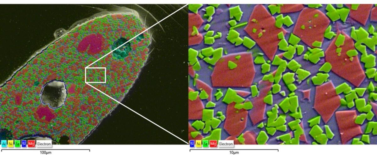
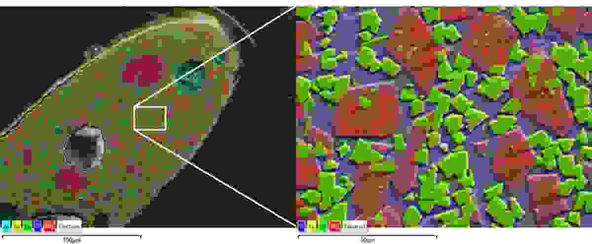
Having found your area of interest, whether it’s something special or just something representative, we can now switch to higher magnification analyses, pushing the limits of SEM-based microanalysis.,For those who haven’t read the previous post, the images below are of a fusion crust m, with a mix of olivine grains (red) enclosing small magnetite (Fe3O4) grain (green) within a silicate-rich glass matrix (blue). The left image shows a quick overview map obtained at 20 kV and ~1,000x magnification. For the right image, I used the exact same detector (Ultim Max 170) but dropped the accelerating potential all the way down to 5 kV and increased the magnification to ~10,000x. This vastly reduced the interaction volume of the incoming electron beam, thus greatly improving the spatial resolution of the EDS analysis. Consequently, you can now see how much clearer the faceted iron oxide and olivine grains are, even where they overlap each other; features which just wouldn’t be clear enough if using 20 kV. It should be noted, however, that when carrying out EDS at lower accelerating potentials, you should collect the maps for longer, to collect more X-rays.
Can we go smaller?
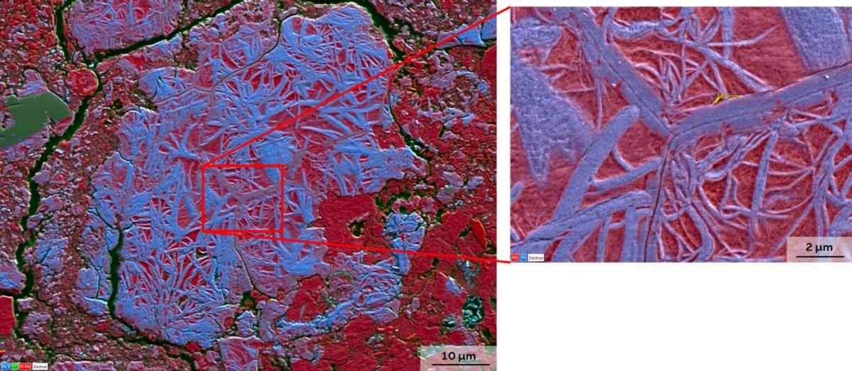
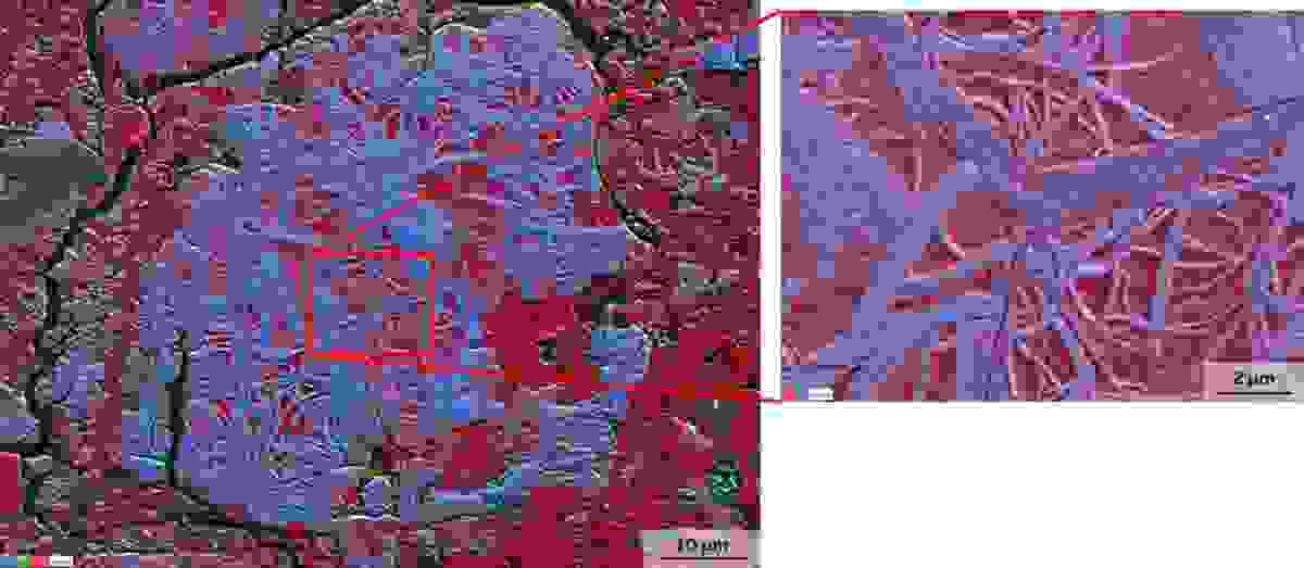
But what if there were features smaller than those seen in the fusion crust, and you still wanted to be able to map the elements present confidently and precisely? The images below show exactly that. The image below is from the same sample (the Winchcombe meteorite), but it shows a highly altered olivine grain which contains an iron-rich fine, serpentine vein structure. The left image is, like before, obtained using the Ultim Max 170 EDS detector at 5 kV, which does show the veins very well. The image on the right image, however, is of a much smaller region obtained using the Ultim Extreme windowless EDS detector at 3 kV. The windowless detector allows for lower energy X-ray lines to be detected and is, therefore, able to use much lower accelerating potentials, consequently increasing the resolution even further down to the nanometre-scale. The right image clearly shows features below 100 nm. Depending on what elements you’re interested in and what X-ray lines you’re needing to excite, you could go right down to 1 kV and really push the spatial resolution of EDS analysis.
Let’s switch things up
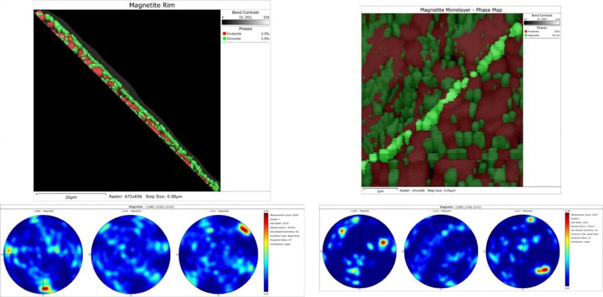
Now we can switch seamlessly to EBSD to investigate the crystal structure and such details relating to grain orientations, deformation, phase distribution, etc. It’s also a great technique to distinguish between polymorphs. Due to the nature of EBSD, including the large tilt angle required for the sample , the resolution can be far greater than when carrying out EDS. Typically you’ll be able to go down to a step size of 25 nm (maybe a little less). The images below show two areas analysed within the fusion core with the top images showing the phase map of olivine (red) and magnetite (green) and the lower images showing the magnetite pole figures. The left map had a pixel size of 80 nm and the right map had a pixel size of 50 nm, with both being collected at 20 kV.
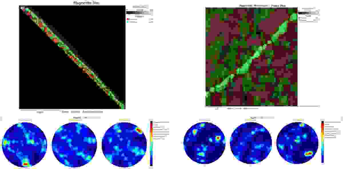
The left shows the outermost rim being comprised of a magnetite layer and the pole figures indicate the {111} planes are aligning with the outermost surface of the fusion crust. The right is of an area within the crust that shows a line of magnetite within the crust rather than the rim, and these magnetite bands have the same {111} plane alignment as for the outer rim in the left image. This may suggest that these lines mark the former outer surface, with subsequent accretion of material of the top.
This shows how EBSD can be used to test hypotheses, even for structure on the nanoscale. To push the resolution even further, a lamella could be produced across this boundary and transmission Kikuchi diffraction (TKD) analysis could be carried out, to achieve step sizes down to ~2 nm; but maybe I’ll leave this for a future blog.
All-in-all…
Don’t forget, from my first post, the importance of sample preparation - without that first stage done properly, you will never achieve the best results. Nevertheless, you’ve seen that it should be relatively easy to get good, high-resolution results by just changing beam conditions.
Give it go, don’t always do what you’ve done before – try something new, try doing some backscatter or EDS at 10 kV to begin and see how the resolution improves.