Webinar
InP Laser Diode Manufacturing


Related to: Semiconductors, Microelectronics and Data Storage
Plasma assisted etch and deposition solutions for the fabrication of devices in a wide range of material systems
With the increase in demand for high-efficiency power conversion in new technologies such as electric cars having high performance is a must. Using materials such as SiC and GaN has lead to lower energy losses. Through atomic layer deposition (ALD) and plasma assisted etch and deposition we are able to optimise processes to deliver the most efficient devices. Our ALD processes reduce threshold voltage shift in GaN/AlGaN devices through excellent passivation.
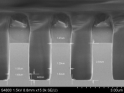
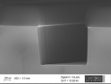
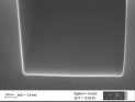
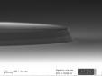
Our etch processes for both GaN and SiC produce excellent quality sidewalls with minimum damage to ensure optimum performance.
With the increase in demand for high-efficiency power conversion in new technologies such as electric cars having high performance is a must. Using materials such as SiC and GaN has lead to lower energy losses. Through atomic layer deposition (ALD) and plasma assisted etch and deposition we are able to optimise processes to deliver the most efficient devices. Our ALD processes reduce threshold voltage shift in GaN/AlGaN devices through excellent passivation.
Our etch processes for both GaN and SiC produce excellent quality sidewalls with minimum damage to ensure optimum performance.
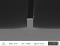
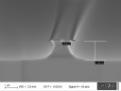
Lasers have a huge array of applications from faster communications to enabling self-driving vehicles through LiDAR. Oxford Instruments has been developing the processes for the III-V materials required in laser diodes for a long time. No matter what the material having ultimate process control is crucial and we have that process from AlGaN to InP.
Process Solutions for Laser Applications
© Oxford Instruments 2026